Thin film capacitor and method of manufacturing the same
a technology of thin film capacitors and film capacitors, which is applied in the direction of fixed capacitors, stacked capacitors, fixed capacitor details, etc., can solve the problems of large leakage current, low reliability, and formation of capacitors with high breakdown voltag
- Summary
- Abstract
- Description
- Claims
- Application Information
AI Technical Summary
Problems solved by technology
Method used
Image

Examples
second example
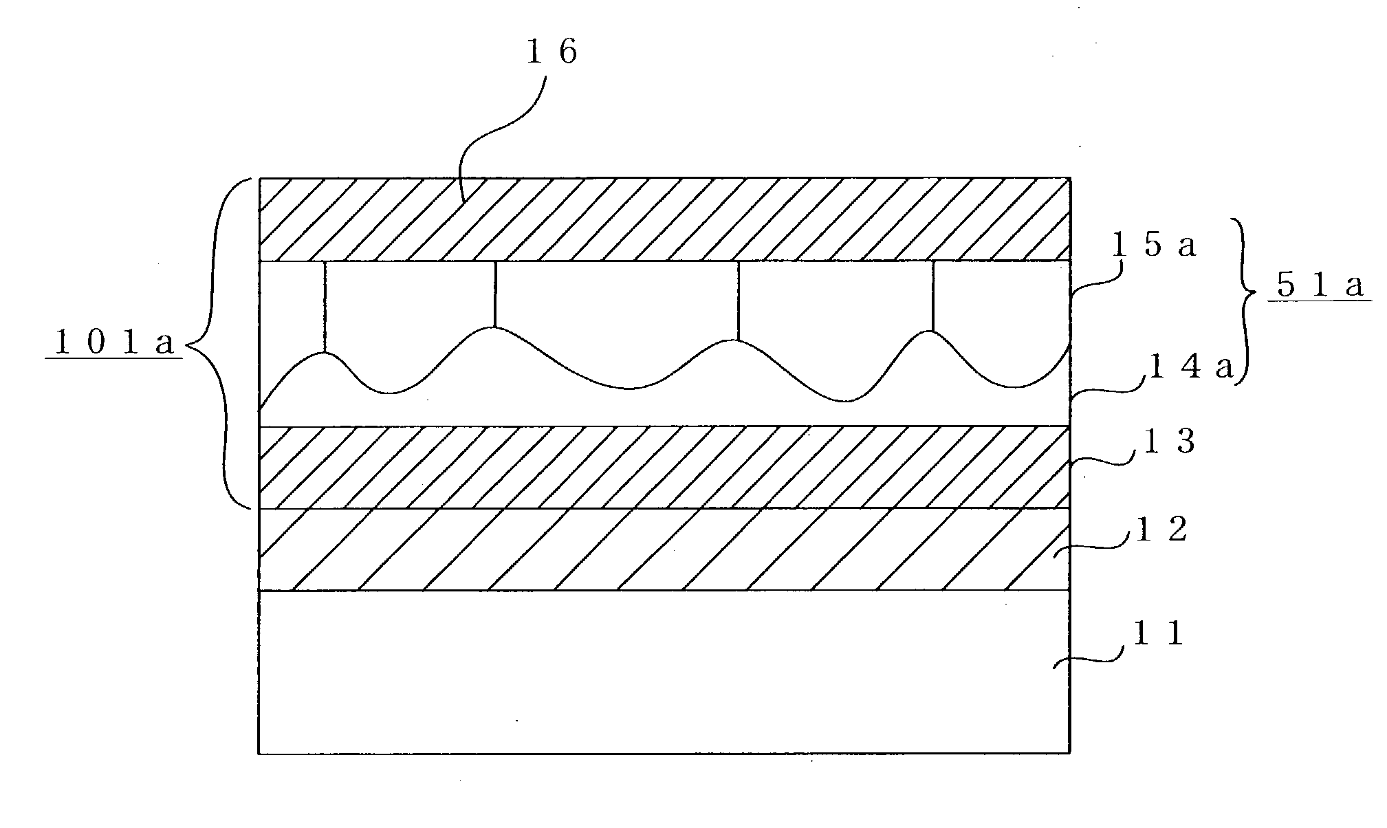
[0078] Next, a structure of the capacitor lO1b as a second example of the present invention will be explained with reference to FIG. 5 hereunder. FIG. 5 is a view showing a sectional structure of the capacitor 1O1b as the second example of the present invention.
[0079] A difference from the first example is that the adhesion enhancing layer 17 was formed between the silicon oxide film 12 on the silicon substrate 11 and the first electrode 13. As the material of the adhesion enhancing layer 17, a TiO.sub.2 film was employed. Then, a further difference from the first example is that a film thickness of the amorphous dielectric film 14b of the capacitor insulating film 51b was formed thin. A minimum film thickness of the amorphous dielectric film 14b was almost 1 nm, and a maximum film thickness thereof was almost 10 nm. The reason why the film thickness of the amorphous dielectric film 14b was formed thin is that, since the substrate heating temperature during the film formation was se...
third example
[0083] Next, a structure of the capacitor 101c as a third example of the present invention will be explained with reference to FIG. 6 hereunder. FIG. 6 is a view showing a sectional structure of the capacitor 101c as the third example.
[0084] Differences from the first example reside in that strontium titanium oxide (STO) was employed as the dielectric material of the capacitor insulating film 51c and the laminated structure in which the amorphous STO film 18 and the polycrystalline STO film 19 were laminated via the wave-like interface was employed as the capacitor insulating film 51c. The film formation of the capacitor insulating film 51c was executed by using the strontium titanium as a target and then sputtering the target by the gas in which O.sub.2 is added to the sputter gas Ar.
[0085] Then, the relative dielectric constant .di-elect cons., the leakage current density J.sub.L (A / cm.sup.2), and the dielectric breakdown field strength E.sub.br (V / cm) of the above capacitor 101c ...
second embodiment
[0089] (Second Embodiment)
[0090] Next, applications of a thin film capacitor according to a second embodiment of the present invention will be explained with reference to FIG. 7, FIG. 8, and FIG. 9 hereinafter. FIG. 7, FIG. 8, and FIG. 9 are sectional views showing the application of the thin film capacitor according to the second embodiment respectively.
[0091] In FIG. 7, two thin film capacitors 101d, 101e are connected in series. Two thin film capacitors 101d, 101e are put on separate conductive film patterns 22a, 22b, which are isolated electrically, respectively and are fixed thereto by the conductive adhesive. In order to connect two thin film capacitors 101d, 101e in series, an upper electrode of one thin film capacitor 101d are connected via a wire 23a to the conductive film pattern 22b, on which the other thin film capacitor 101e is put and which is connected to a lower electrode of thereof.
[0092] In FIG. 8, two thin film capacitors 101f, 101g are connected in parallel. Two ...
PUM
| Property | Measurement | Unit |
|---|---|---|
| Thickness | aaaaa | aaaaa |
| Thickness | aaaaa | aaaaa |
| Thickness | aaaaa | aaaaa |
Abstract
Description
Claims
Application Information
 - R&D
- Intellectual Property
- Life Sciences
- Materials
- Tech Scout
- Unparalleled Data Quality
- Higher Quality Content
- 60% Fewer Hallucinations
Browse by: Latest US Patents, China's latest patents, Technical Efficacy Thesaurus, Application Domain, Technology Topic, Popular Technical Reports.
© 2025 PatSnap. All rights reserved.Legal|Privacy policy|Modern Slavery Act Transparency Statement|Sitemap|About US| Contact US: help@patsnap.com