

Semiconductor device, manufacturing thereof and power amplifier module
a technology of semiconductor devices and power amplifier modules, which is applied in the direction of high-frequency amplifiers, bulk negative resistance effect devices, solid-state devices, etc., can solve the problems of increased cost of semiconductor devices, difficulty in realizing r2.5, and increased mismatch with matching circuits in view of high frequency
- Summary
- Abstract
- Description
- Claims
- Application Information
AI Technical Summary
Benefits of technology
Problems solved by technology
Method used
Image

Examples
embodiment 1
[0079] Embodiment 1
[0080] A description will below be made of an emitter top HBT which is a first embodiment of the invention in reference to FIG. 1, FIG. 11, FIG. 12 and FIG. 13.
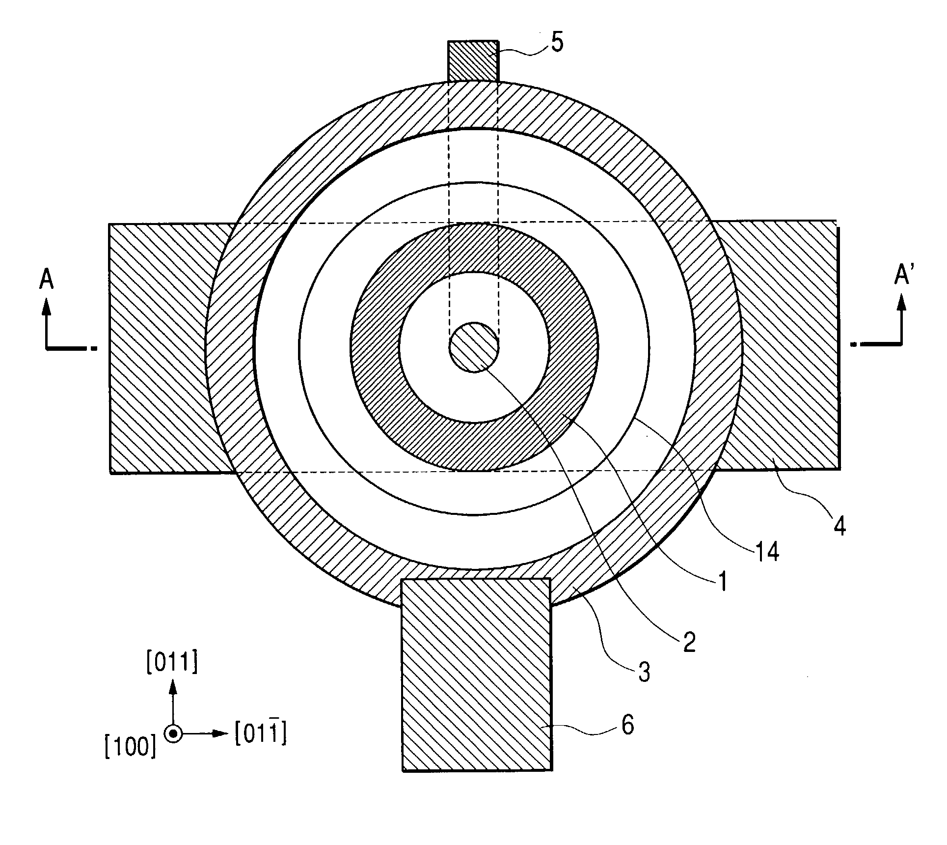
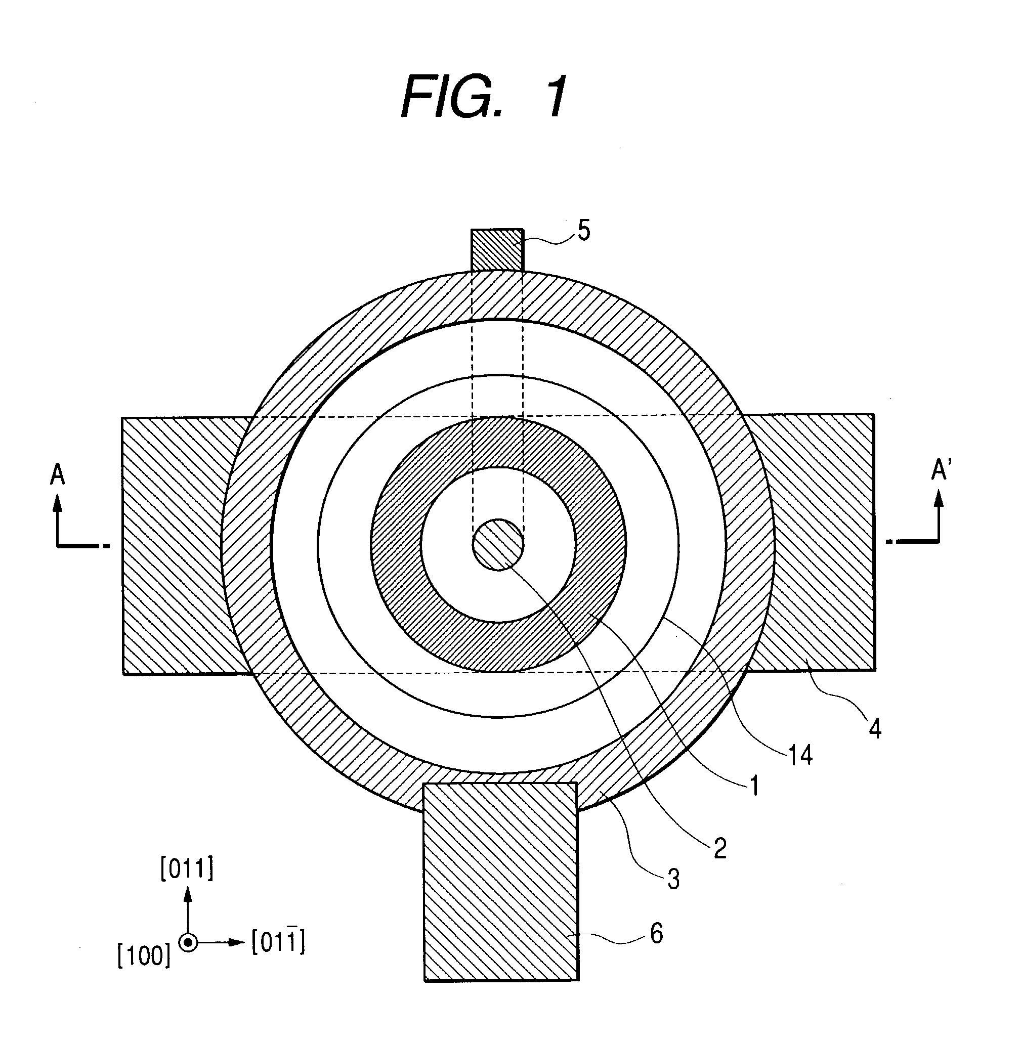
[0081] FIG. 1 is a plan structure view of an emitter top HBT which is a first embodiment of the invention. A base electrode 2 is arranged on an inner side of a ring-like emitter electrode 1 and a collector electrode 3 is arranged on an outer side thereof. Further, emitter wiring 4 (not illustrated on an inner side of the collector electrode 3), base wiring 5 (not illustrated on the inner side of the collector electrode 3) and collector wiring 6 are connected to the emitter electrode 1, the base electrode 2 and the collector electrode 3 respectively via through holes (not illustrated). The ratio r is determined by a distance between a base mesa outer periphery 14 and the emitter electrode 1 and when 1.0 .mu.m is considered as matching allowance of photolithography, in the case of the emitter electrode having...
embodiment 2
[0087] Embodiment 2
[0088] An explanation will below be given of an emitter top HBT which is a second embodiment of the invention in reference to FIG. 1, FIG. 2, FIG. 4, FIG. 5 and FIG. 6.
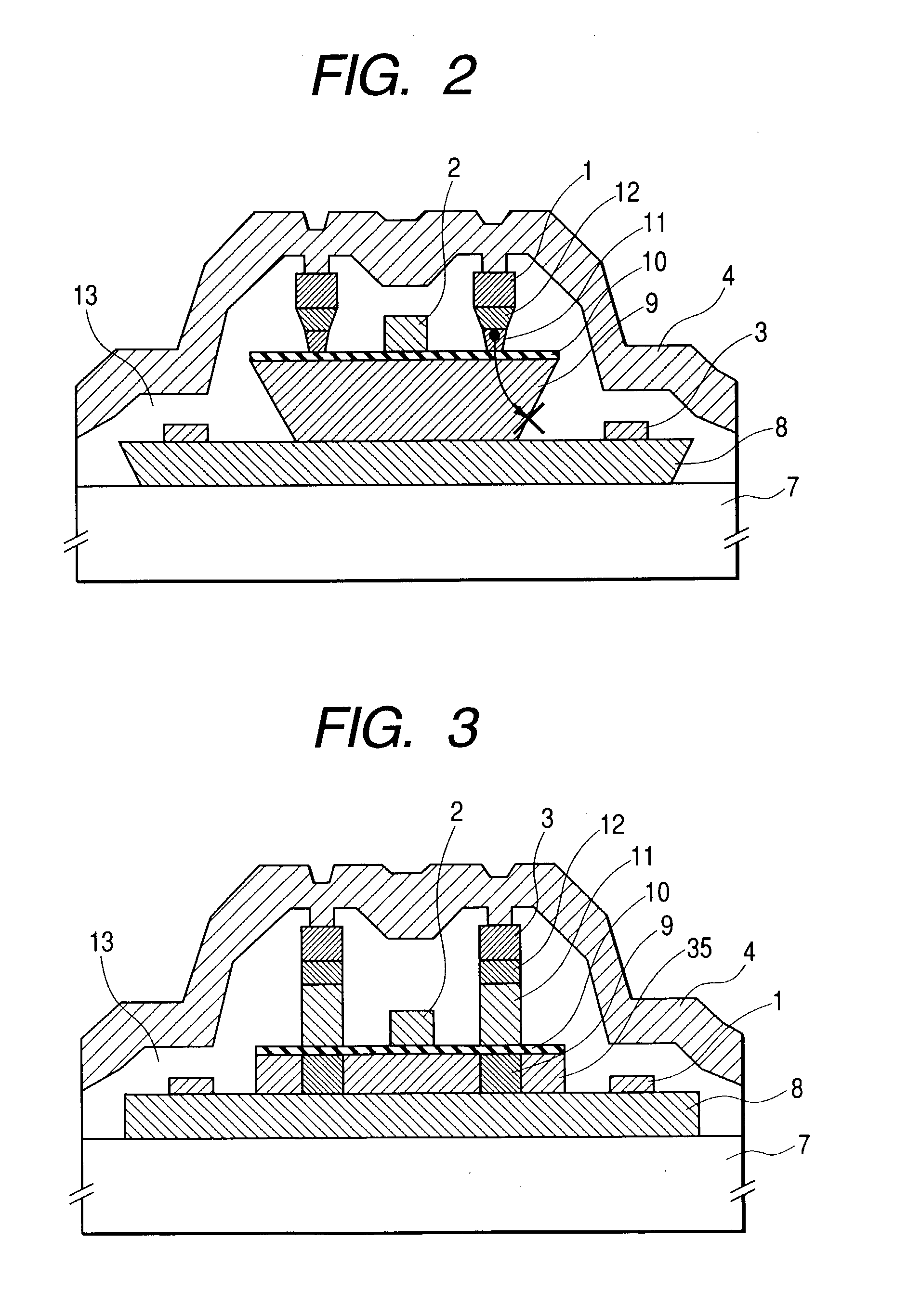
[0089] FIG. 4 is a plan structure view of the emitter top HBT which is the second embodiment of the invention. When in the ring-like emitter HBT shown in Embodiment 1 (FIG. 1), the match allowance between the base mesa outer periphery 14 and the emitter electrode 1 is reduced to 0.5 .mu.m to realize r<2.0, at a face taken along line A-A' of FIG. 1, as shown by FIG. 2, an inverse mesa shape appears at the base mesa outer periphery 14. Since the match allowance between the base mesa outer periphery 14 and the emitter electrode 1 is small, the GaAs surface having a high recombination rate is present within a distance of diffusing electrons at the inside of the collector and the current gain is deteriorated. Hence, as shown by FIG. 4, a side in parallel with [011] direction in which the inverse mesa sha...
embodiment 3
[0093] Embodiment 3
[0094] An explanation will below be given of an emitter top HBT which is a third embodiment of the invention in reference to FIG. 7.
[0095] FIG. 7 is a plan structure view of the emitter top HBT which is the third embodiment of the invention. Although a side in parallel with [011] direction is present, a minimum value of a distance between an outer periphery of a base / collector junction region and an outer periphery of an emitter / base junction region of HBT in [01-1] direction becomes larger than a minimum value of the distance in [011] direction. Specifically, match allowance between the base mesa outer periphery 14 and the emitter electrode 1 is set to 0.5 .mu.m in [011] direction and 1.5 .mu.m in [01-1] direction. Further, wet etching is used in fabricating HBT similar to Embodiment 2.
[0096] According to the invention, in a semiconductor device using an emitter top type HBT formed above a zinc blende type semiconductor substrate having a (100) (.+-.5 degrees) fa...
PUM
 Abstract
Description
Claims
Application Information