Method for producing micro probe tips

a micro-probe tip and tip technology, applied in the direction of resistive material coating, printed circuit assembling, metallic material coating process, etc., can solve the problems of wasting time and money when bad dies are packaged, manufacturing wafers consume the most time in the process of manufacturing ic products, and the cost of testing is an important component of the total cost of producing ics

Inactive Publication Date: 2003-12-04
SCS HIGHTECH
View PDF13 Cites 17 Cited by
  • Summary
  • Abstract
  • Description
  • Claims
  • Application Information

AI Technical Summary

Problems solved by technology

Besides, the cost of testing is an important component of the total cost of producing ICs.
Such a process does not sort out bad dies before packaging and thus wastes time and money when bad dies are packaged.
Manufacturing wafers consumes the most time in the process of manufacturing IC products.
It is consequently normal to produce a number of surplus wafers at the first stage of IC production in anticipation of failures because it is generally not acceptable to start replacement wafer production when the IC failure rate is known.
The result is that a manufacturer will keep a larger stock of wafers on hand, which increases costs.
In a multi-chip module any bad chip will result in the discard of the entire module.
The testing thus experiences the greater complexity of the module and achieves less reliable results.
The result is higher testing costs, longer research and development cycles and costs, and a higher ri...

Method used


Image

  • Method for producing micro probe tips
  • Method for producing micro probe tips
  • Method for producing micro probe tips

Examples


Embodiment Construction

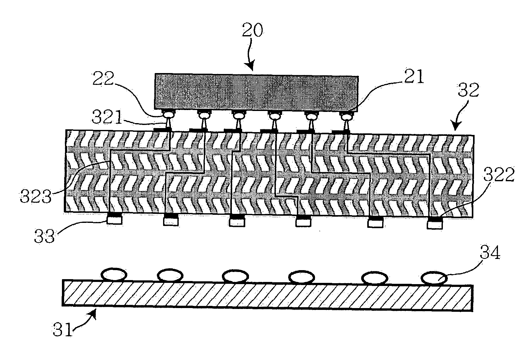
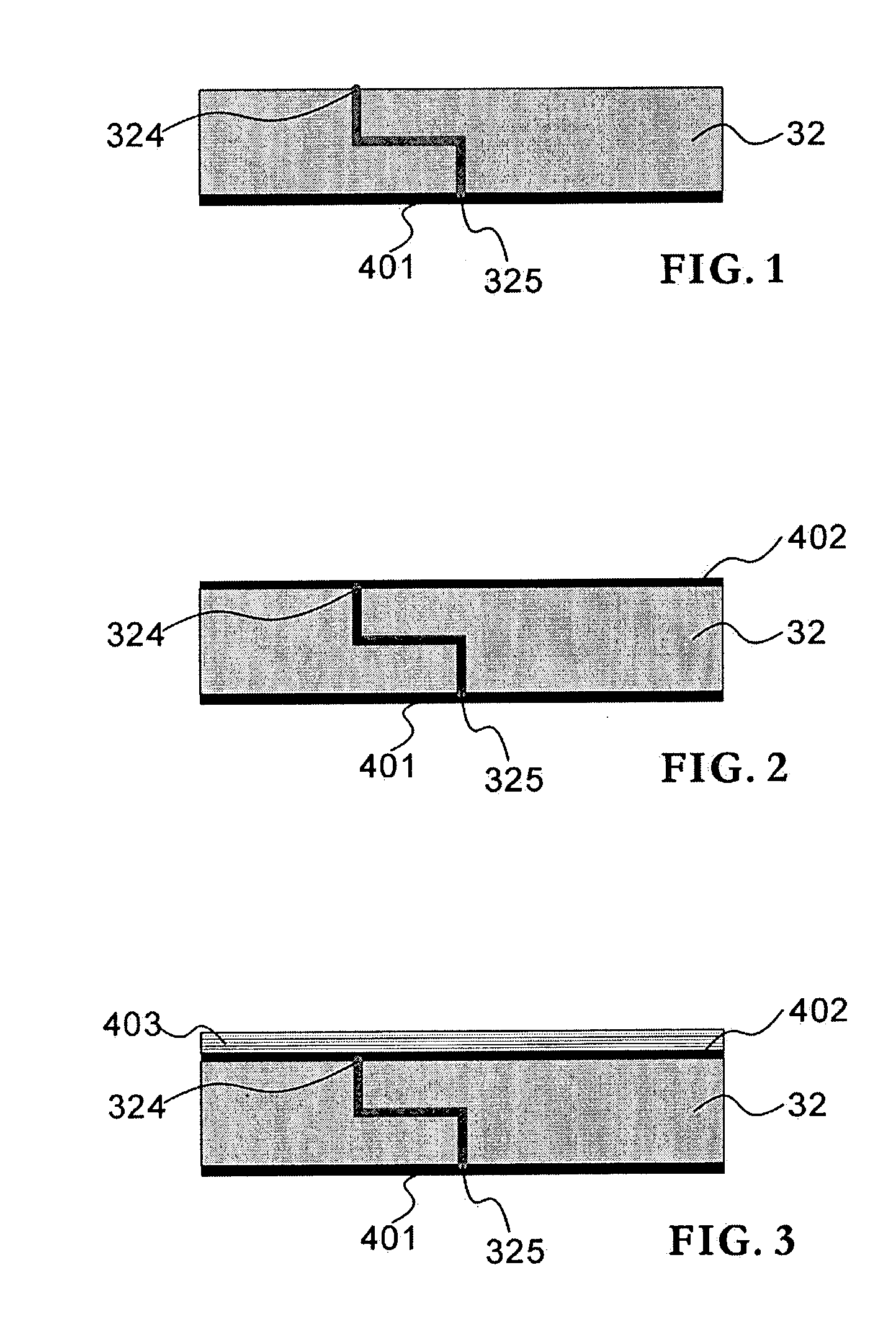
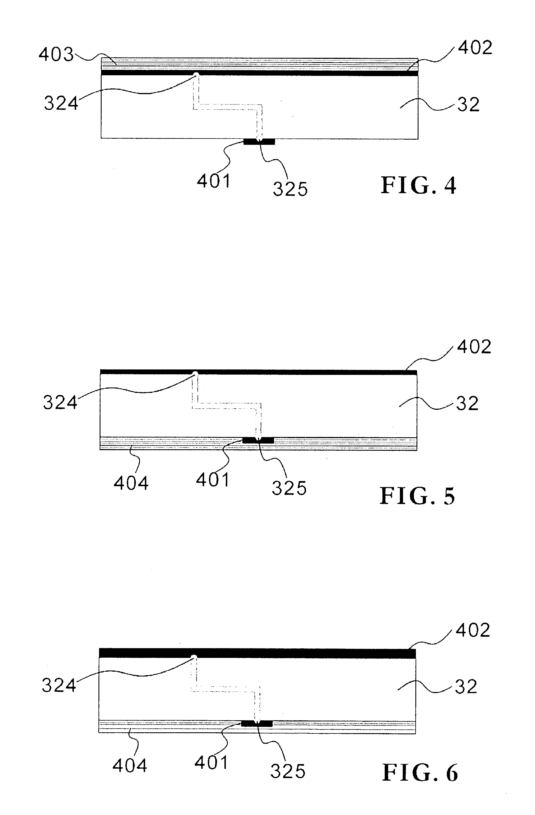
[0011] An aspect of the present invention provides a method for producing a plurality of stiff vertical micro probes on a probe card adapted for accurately testing integrated circuit devices with high frequency signals.

[0012] Another aspect of the present invention provides a method for producing a large number of stiff vertical micro probes on a probe card adapted for testing integrated circuit devices with reduced sizes or with denser I / O terminals.

[0013] Still another aspect of the present invention provides a method for producing a large number of stiff vertical micro probes on a probe card adapted for testing integrated circuit devices having I / O terminals distributed over circumference and the central area of an IC die adapted for mounting to a printed circuit board using flip chip technologies.

[0014] Still another aspect of the present invention provides a method for producing a large number of stiff vertical micro probes on a probe card that is durable and has a simple struc...


PUM

PropertyMeasurementUnit
Circumferenceaaaaaaaaaa
Surface areaaaaaaaaaaa
Conductionaaaaaaaaaa

Abstract

Micro-fabrication forms a plurality of stiff vertical micro probes on the front surface of a ceramic substrate and a plurality of contacts on the back surface of the ceramic substrate. Photolithography, various etching technologies and electroplating are used to form the micro probes on the surface of the ceramic substrate. The produced micro probes are mechanically strong and consequently have a long duty life. Moreover, the probes can be arranged into a high-density planar array to conform to the newest integrated circuit devices which have dense I/O terminal arrays.

Description

PRIORITY[0001] This application claims priority from Taiwanese patent application 091104650, filed Mar. 13, 2002, which application is incorporated by reference in its entirety.[0002] 1. Field of the Invention[0003] The present invention relates to a method for producing probe cards for testing integrated circuits, more particularly the process for forming micro probes on a ceramic substrate for testing integrated circuits, and also to the process for testing one or more dies on an integrated circuit wafer using such a probe card.[0004] 2. Description of the Related Art[0005] Testing integrated circuit ("IC") characteristics including reliability of ICs is indispensable to the semiconductor industry. As IC manufacturing technology advances, ICs perform better and are able to work at higher frequencies with ever smaller die sizes. The technology and equipment for IC testing needs to advance correspondingly. The number and density of the probes on a testing probe card should conform w...

Claims


Application Information

Patent Timeline
IPC IPC(8): G01R3/00H05K3/24H05K3/40
CPCG01R3/00H05K3/243Y10T29/49155Y10T29/4913Y10T29/49204H05K3/4007
Inventor HUNG, WEN-CHINGHSU, HOWARD
Owner SCS HIGHTECH
Why Eureka
Try Eureka