Light emitting device and manufacturing method thereof

a technology of light emitting devices and manufacturing methods, applied in the direction of organic light emitting devices, semiconductor devices, electrical devices, etc., can solve the problems of high film resistance of transparent electrodes and restricted opening ratios

Inactive Publication Date: 2003-12-11
SEMICON ENERGY LAB CO LTD
View PDF99 Cites 176 Cited by
  • Summary
  • Abstract
  • Description
  • Claims
  • Application Information

AI Technical Summary

Benefits of technology

[0013] A problem of the top emission structure is that its transparent electrode has high film resistance. The film resistance becomes even higher when the thickness of the transparent electrode is reduced. When the transparent electrode that serves as a cathode (or an anode) is high in film resistance, a voltage drop makes the intra-plane electric potential distribution uneven and the luminance becomes fluctuated among light emitting elements. Another object of the present invention is therefore to provide a light emitting device structured so as to lower the film resistance of a transparent electrode in a light emitting element, as well as a method of manufacturing the light emitting device. Still another object of the present invention is to provide an electric appliance that uses this light emitting device as its display unit.
[0015] In the present invention, emitted light in the lateral direction is reflected or collected at an inclined surface formed in the first electrode to increase the amount of emitted light taken out in one direction (direction passing through the second electrode).
[0018] Further, the inclined surface formed in the first electrode prevents emitted light from the light emission device (also including emitted light in the lateral direction) from reaching a TFT.
[0039] Further, in accordance with the invention, the shape of an insulator (referred to bank, partition wall, barrier wall, etc.) disposed between each of pixels is improved for eliminating coverage failure, etc. upon forming an layer containing an organic conpound layer comprising a polymeric material by a coating method. In each of the constitutions described above, the upper end of the insulator is provided with a curved surface having a radius of curvature, and the radius of curvature is from 0.2 .mu.m to 3 .mu.m. Further, the tapered angle for the insulator may be 35.degree. to 70.degree..
[0040] By the provision of the radius of curvature, the step coverage is enhanced and a layer containing an organic compound to be formed subsequently can be formed even when it is extremely thin.

Problems solved by technology

There has been a problem in the structure that an opening ratio is restricted depending on an arrangement of TFT and wirings in a pixel portion when definition is to be improved.
For example, light emitted in the lateral direction (the direction parallel to the substrate face) is not taken out and therefore is a loss.
A problem of the top emission structure is that its transparent electrode has high film resistance.

Method used


Image

  • Light emitting device and manufacturing method thereof
  • Light emitting device and manufacturing method thereof
  • Light emitting device and manufacturing method thereof

Examples


embodiment 1

[0140] Embodiment 1

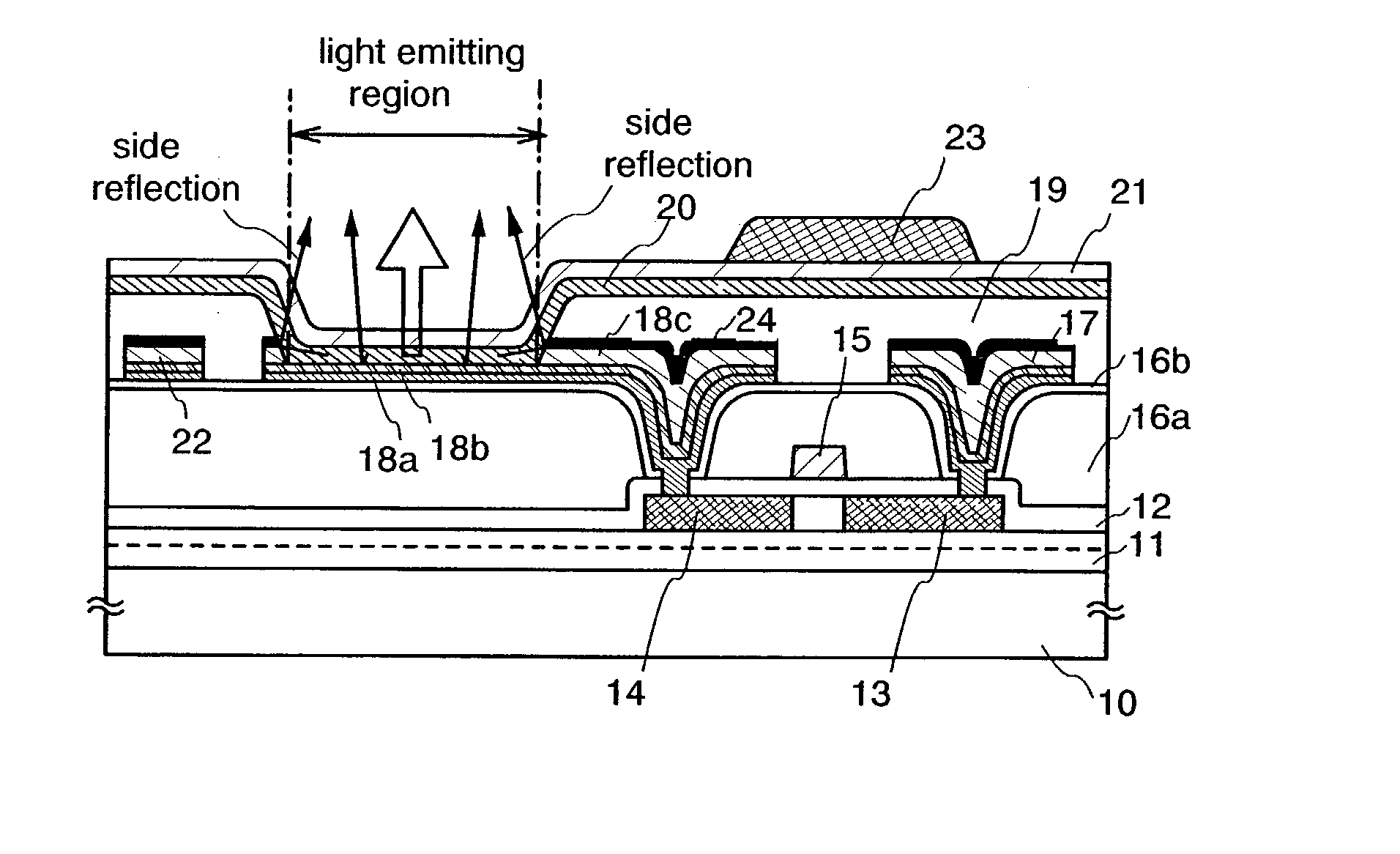
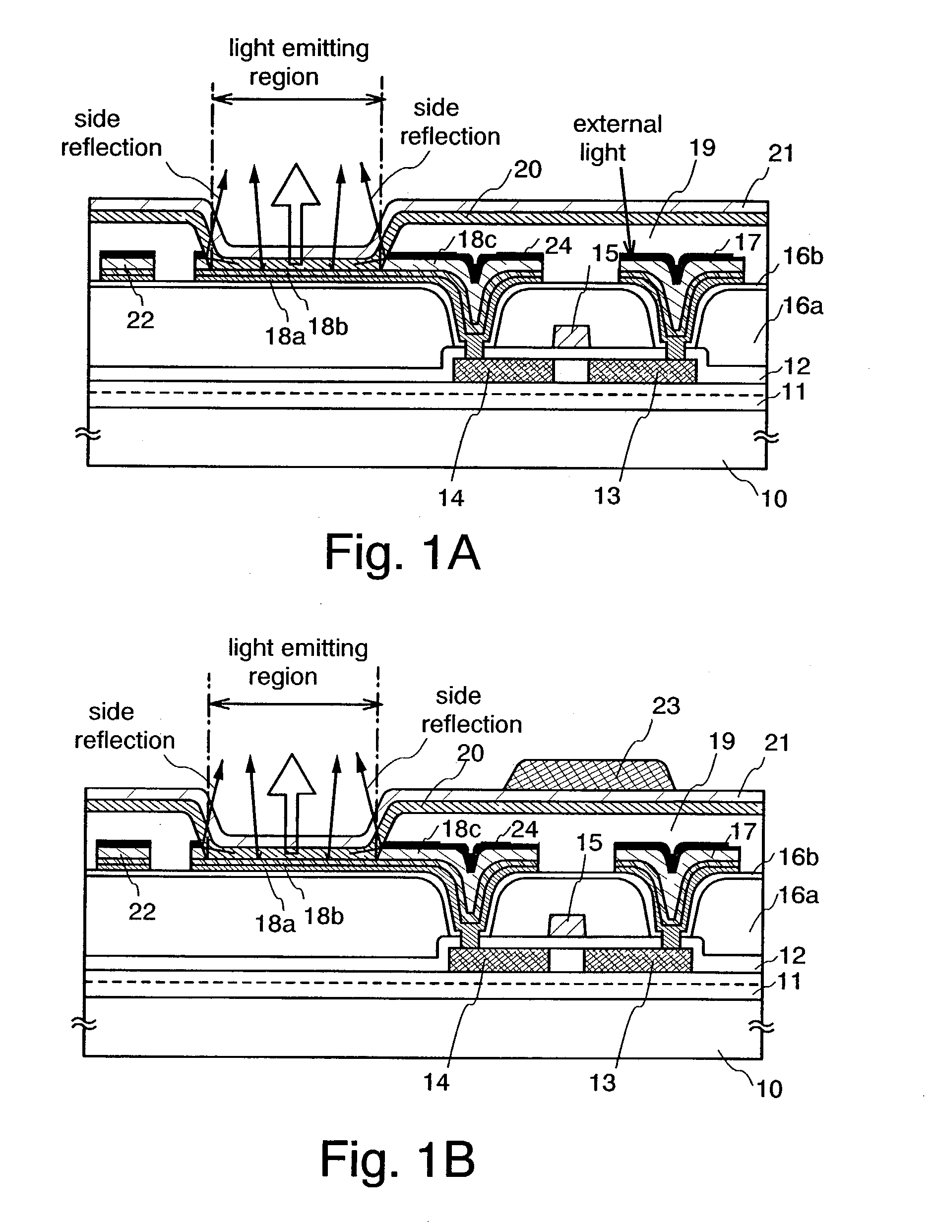
[0141] In this embodiment, a brief description is given with reference to FIGS. 2A to 3C on an example of procedure of forming a light emitting element in accordance with the present invention.

[0142] First, a base insulating film 31 is formed on a substrate 30 which has an insulating surface.

[0143] The base insulating film 31 is a laminate and the first layer is a silicon oxynitride film formed to have a thickness of 10 to 200 nm (preferably 50 to 100 nm) by plasma CVD using as reaction gas SiH.sub.4, NH.sub.3, and N.sub.2O. Here, a silicon oxynitride film (composition ratio: Si=32%, O=27%, N=24%, H=17%) with a thickness of 50 nm is formed. The second layer of the base insulating film is a silicon oxynitride film formed to have a thickness of 50 to 200 nm (preferably 100 to 150 nm) by plasma CVD using as reaction gas SiH.sub.4 and N.sub.2O. Here, a silicon oxynitride film (composition ratio: Si=32%, O=59%, N=7%, H=2%) with a thickness of 100 nm is formed. Although...

embodiment 2

[0165] Embodiment 2

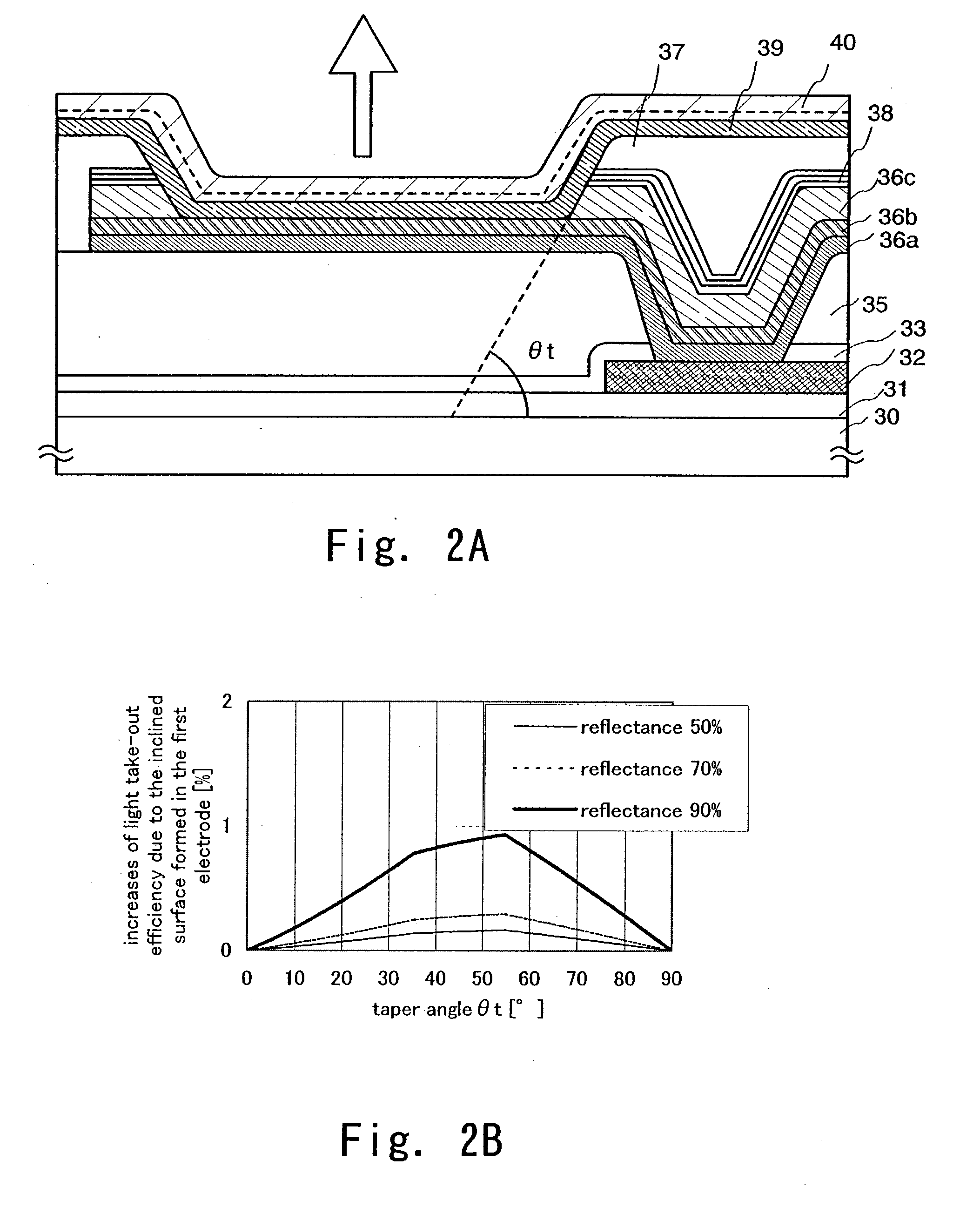
[0166] This embodiment describes with reference to FIGS. 6A to 8 an example of a light emitting device in which an auxiliary electrode is formed.

[0167] FIG. 6A is a top view of a pixel and a sectional view taken along the dot-dash line A-A' is FIG. 6B.

[0168] In this embodiment, steps up through formation of an insulator 67 are identical with those in Embodiment 1 and descriptions thereof are omitted here. The insulator 37 in FIG. 2B corresponds to the insulator 67 in FIG. 6B.

[0169] Following the descriptions in Embodiment 1, a base insulating film, a drain region 62, a gate insulating film 63, an interlayer insulating film 65, layers 66a-c of a first electrode, a light absorbing multi-layered film 61, and the insulator 67 are formed on a substrate having an insulating surface.

[0170] Next, a layer containing an organic compound 68 is selectively formed. This embodiment employs evaporation using an evaporation mask or ink jet to selectively form the layer containing...

embodiment 3

[0178] Embodiment 3

[0179] Further, an exterior view of an active matrix type light emitting apparatus is described with reference to FIG. 9. Further, FIG. 9A is a top view showing the light emitting apparatus and FIG. 9B is a cross-sectional view of FIG. 9A taken along a line A-A'. Reference numeral 901 indicated by a dotted line designates a source signal line driver circuit, numeral 902 designates a pixel portion, and numeral 903 designates a gate signal line driver circuit. Further, numeral 904 designates a seal substrate, numeral 905 designates a first seal agent and an inner side surrounded by the first seal agent 905 constitutes a second agent 907.

[0180] Further, reference numeral 908a, b designates a wiring for transmitting signals inputted to the source signal line driver circuit 901 and the gate signal line driver circuit 903 for receiving a video signal or a clock signal from FPC (flexible printed circuit) 909 for constituting an external input terminal. Further, although ...


PUM


Abstract

A light emission device manufactured by a method of forming a curved surface having a radius of curvature to the upper end of an insulator 19, exposing a portion of the first electrode 18c to form an inclined surface in accordance with the curved surface, and applying etching so as to expose the first electrode 18b in a region to form a light emission region, in which emitted light from the layer containing the organic compound 20 is reflected on the inclined surface of the first electrode 18c to increase the total take-out amount of light in the direction of an arrow shown in FIG. 1A and, further, forming a light absorbing multi-layered film 24 comprising light absorbing multi-layered film on the first electrode 18c other than the region to form the light emission region, thereby obtaining a light emission device of a structure increasing the amount of light emission taken out in one direction in a light emission element, while not all the light formed in the layer containing the organic compound are taken out from the cathode as a transparent electrode toward TFT but the light was emitted also, for example, in the lateral direction (direction parallel with the plane of the substrate).

Description

[0001] 1. Field of the Invention[0002] The present invention relates to a light emitting device with a light emitting element that emits fluorescent light or phosphorescent light upon application of electric field to a pair of electrodes of the element which sandwich a layer containing an organic compound, and to a method of manufacturing the light emitting device. In this specification, the term light emitting device includes an image display device, a light emitting device and a light source (including illuminating device). Also, the following modules are included in the definition of the light emitting device: a module obtained by attaching to a light emitting device a connector such as an FPC (flexible printed circuit; terminal portion), a TAB (tape automated bonding) tape, or a TCP (tape carrier package); a module in which a printed wiring board is provided at an end of the TAB tape or the TCP; and a module in which an IC (integrated circuit) is directly mounted to a light emit...

Claims


Application Information

Patent Timeline
Patent Type & Authority Applications(United States)
IPC IPC(8): H01L27/32H01L51/52
CPCH01L27/3244H01L27/3246H01L51/5206H01L2251/56H01L51/5284H01L51/5203H01L51/56H01L51/5271H10K59/122H10K59/12H10K50/813H10K50/818H10K50/856H10K50/865H10K71/00H10K50/805H10K50/81
Inventor YAMAZAKI, SHUNPEINODA, TAKESHIHIGAKI, YOSHINARI
Owner SEMICON ENERGY LAB CO LTD
Why Eureka
Try Eureka