Control circuit for charging and discharging, illuminating apparatus and driving method thereof

Active Publication Date: 2003-12-11
NICHIA CORP
View PDF5 Cites 18 Cited by
  • Summary
  • Abstract
  • Description
  • Claims
  • Application Information

AI Technical Summary

Problems solved by technology

However, there is a problem that electric charge remains in light-emitting diodes (light-emitting elements) connected to the common source line, which is not selected, or light-off status, while the light-emitting diodes (light-emitting elements), which are connected to the selected common source line, emit.
Such a residual charge, which remains in the unselected period, produces an undesirable current when the common source line is selected.
Such produced undesirable current reduces display quality because of undesirable-emission that the light-emitting diode, which is controlled not emitting, slightly emits, and insufficient contrast in display image.
Therefore, the circuit cannot prevent the undesirable-emission that the light-emitting diode, which is controlled not emitting, slightly emits.
For example, there is the same problem in voltage control elements in a liquid crystal display.
Especially, in a large-scale display with long traces or numbers of traces, there is a problem such as an undesirabl

Method used


Image

  • Control circuit for charging and discharging, illuminating apparatus and driving method thereof
  • Control circuit for charging and discharging, illuminating apparatus and driving method thereof
  • Control circuit for charging and discharging, illuminating apparatus and driving method thereof

Examples


embodiment 2

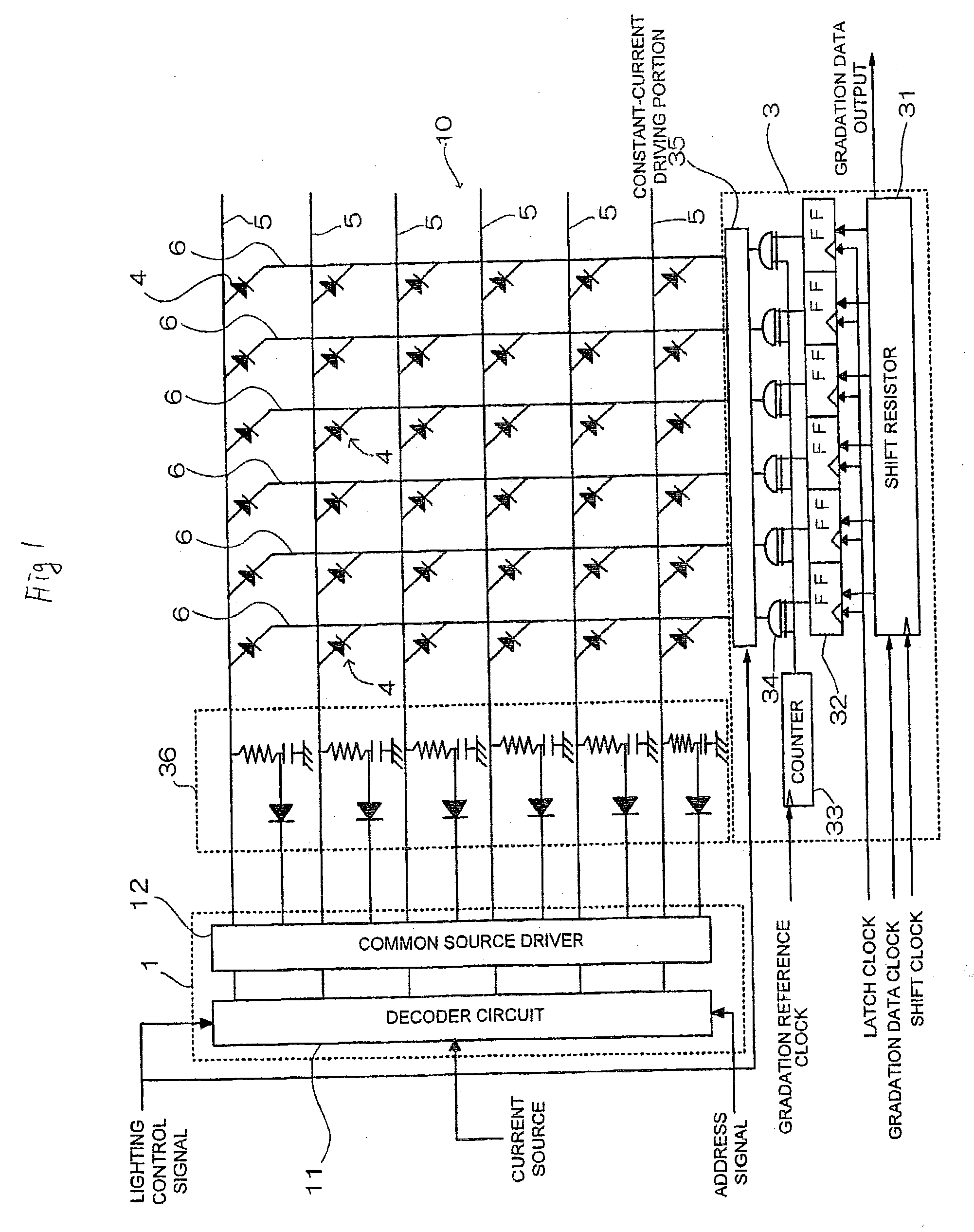
[0156] The following description will describe the second embodiment according to the present invention with reference to the drawings. FIG. 7 to FIG. 10 show a second driving method according to the present invention. The second driving method is an embodiment, in which a residual charge in a current line is eliminated when scanning changes into the next common switch line.

[0157] In FIG. 7 to FIG. 10, current lines (driving lines), common switch lines (scanning lines), charge elements connected at locations corresponding to intersections of them, a common switch line scanning circuit, a current line driving circuit, an anode control circuit for charging and discharging, and a driving control circuit are shown as A.sub.1-A.sub.256, B.sub.1-B.sub.64, E.sub.1,1-E.sub.256,64, 41, 42, 43, and 44 respectively.

[0158] The common switch line scanning circuit 41 has scanning switches 45.sub.1-45.sub.64 for sequentially scanning common switch lines B.sub.1-B.sub.64. One terminal of each of th...

embodiment 3

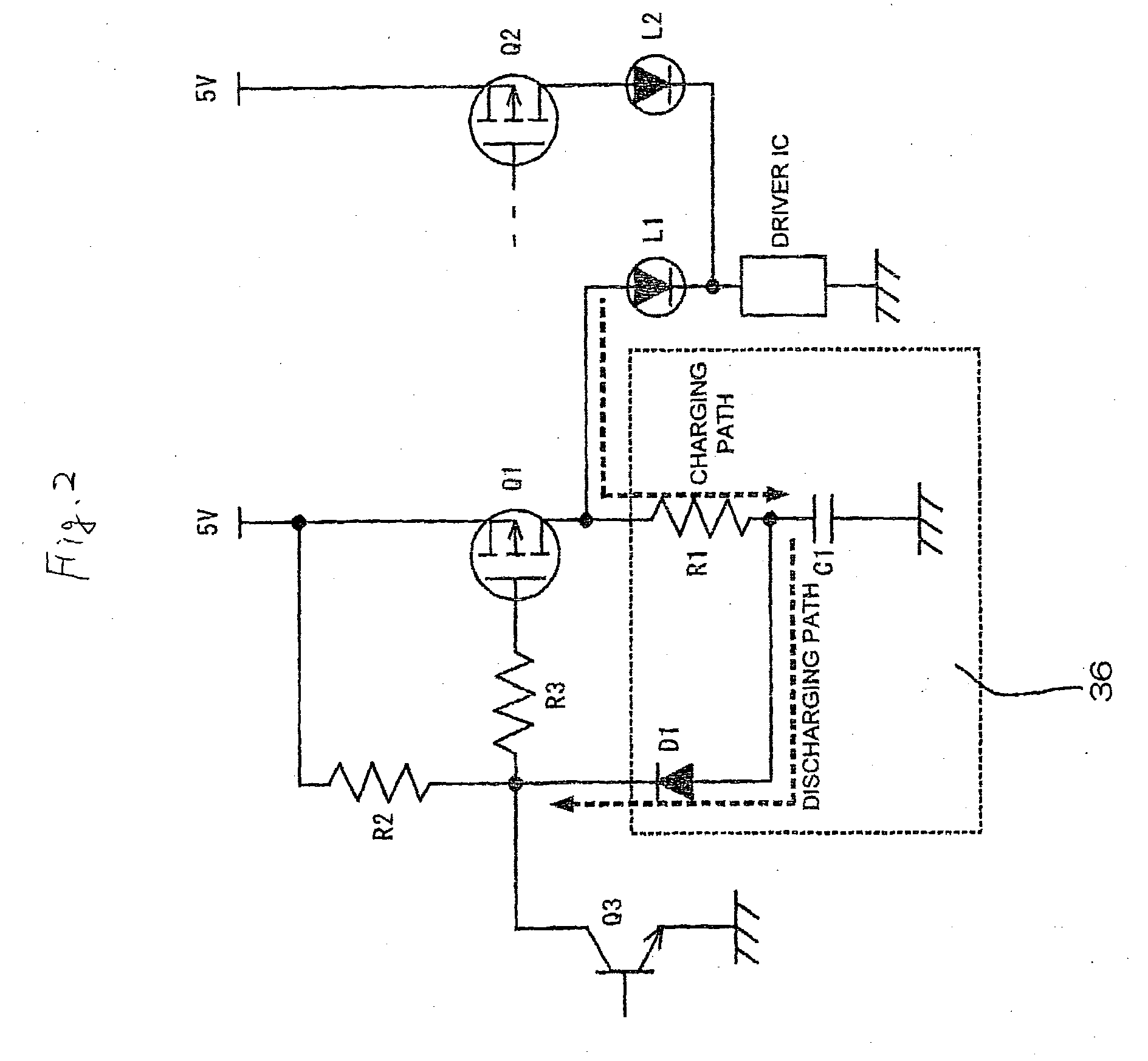
[0181] The following description will describe an undesirable-emission-pre-venting circuit of a control circuit for charging and discharging of the embodiment 3 according to the present invention with reference to FIG. 12.

[0182] In FIG. 12, a switch (SW2) operates in synchronization with a switch (SW1). When the switch (SW1) is connected to a power supply (5V), the switch (SW2) is opened, and when the switch (SW1) is grounded, the switch (SW2) is grounded. In addition, when the switch (SW1) is grounded, a transistor (Q1) is turned on, and a light-emitting diode (L1) emits corresponding to a driving status of a driver IC. At this time, the switch (SW2) is grounded, and a residual charge accumulated in a capacitor (C1) is discharged through the switch (SW2).

[0183] When the switch (Sw1) is connected to the power supply (5V), the transistor (Q1) is turned off, and the light emitting diode (L1) is in a driven-off status irrespective of a driving status of the driver IC. While a transisto...

embodiment 4

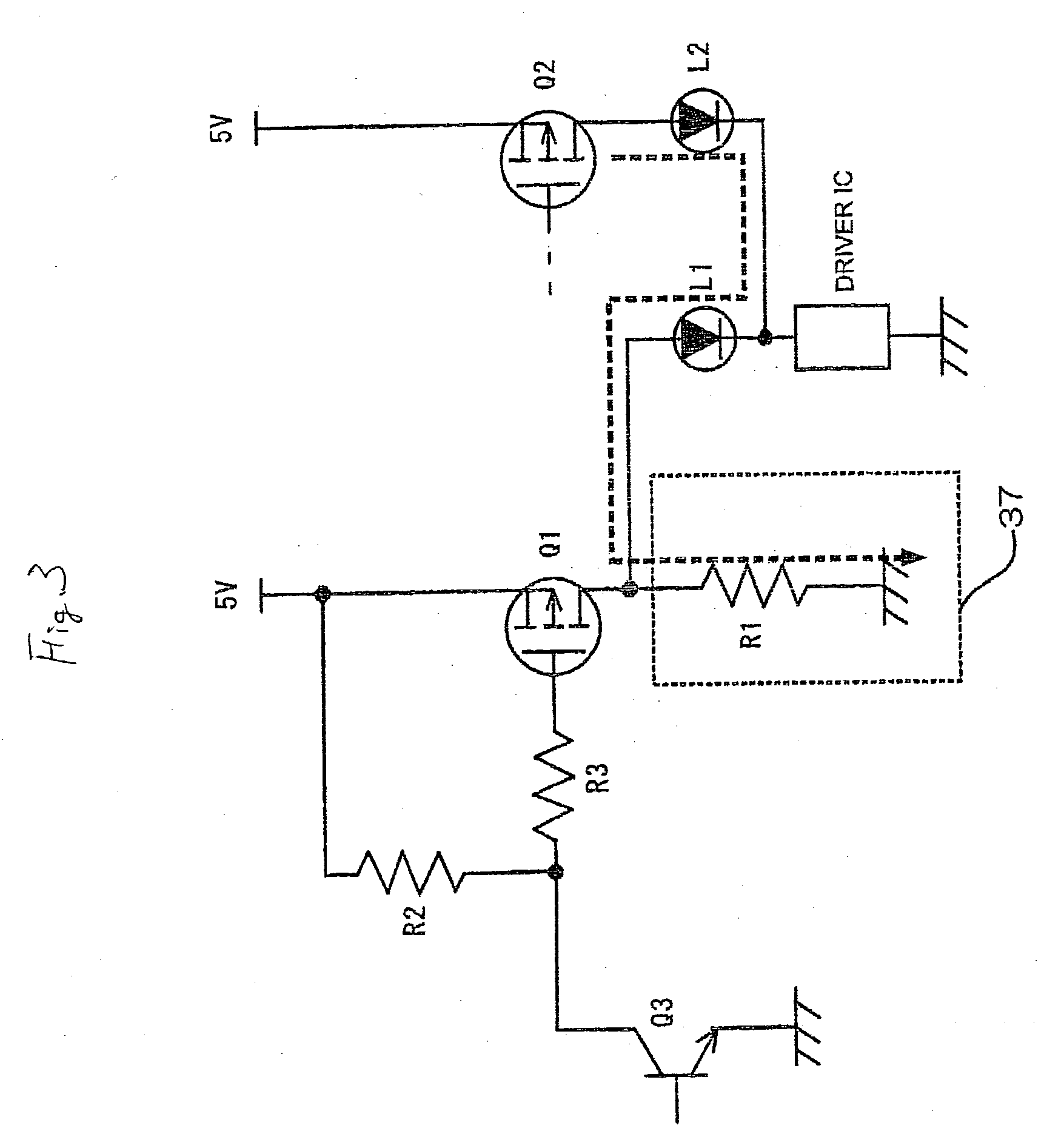
[0187] The following description will describe an undesirable-emission-pre-venting circuit of a charging-and-discharging preventing circuit of the embodiment 4 according to the present invention with reference to FIG. 13. In the undesirable-emission-preventing circuit according to this embodiment, the switch (SW2) in the undesirable-emission-preventing circuit according to the embodiment 3 is eliminated, and the capacitor (C1) is connected to the switch (SW1) via the diode (D1). Only control of the switch (SW1) operates as the undesirable-emission-preventing circuit of the embodiment 3. FIG. 13 is a circuit diagram, which is simplified based on the circuit in FIG. 2. The operation will be briefly described as follows.

[0188] In addition, when the switch (SW1) is grounded, the transistor (Q1) is turned on, and the light-emitting diode (L1) emits corresponding to a driving status of the driver IC. At this time, the charge accumulated in the capacitor (C1) is discharged via a path from ...


PUM


Abstract

It is an object of the present invention to provide a control circuit for charging and discharging (43) etc., which can prevent an undesirable-emission caused by a residual charge, capable of obtaining a high-quality display and so on. The control circuit for charging and discharging (43) includes a driven element (E1,1-E256,64) with a driving-on status and a driving-off status; a charging element, whose one end is grounded; and a driving circuit (44), which is connected to the driven element (E1,1-E256,64), for controlling the driving-on status or the driving-off status in the driven element. The control circuit further includes a charging path, which is connected to the driven element (E1,1-E256,64), for charging the charging element with a residual charge, which is produced in the driven element (E1,1-E256,64) and/or a line connected to the driven element (E1,1-E256,64) during the driving-on status, and a discharging path, which is connected to the charging path, for discharging the residual charge from the charging element to a ground in the driving-on status.

Description

[0001] This application is based on Application No. 2002-142432 filed in Japan on May 17, 2002, and No. 2003-107044 filed in Japan on Apr. 10, 2003, the contents of which are incorporated hereinto by references.[0002] 1. Field of the Invention[0003] The present invention relates to a control circuit for charging and discharging, an illuminating apparatus and a driving method thereof, which control charging and discharging in an illuminating apparatus with a display portion composed of driven elements such as liquid crystal display or a plurality of light-emitting elements and so on.[0004] 2. Discussion of the Related Art[0005] Recently, more than 1000 mcd of high-luminance light-emitting diodes have been developed for each of RGB, and production of large-scale LED display is started. The LED displays have characteristics that they can be lightweight and thinned, and they consume less power, etc. Hence, a demand for the LED displays as large-scale displays that can be used outdoors h...

Claims


Application Information

Patent Timeline
IPC IPC(8): G09G3/20G09G3/22G09G3/32H01L33/00
CPCG09G3/22G09G3/3216G09G2320/02G09G2310/0251G09G2310/0275G09G3/3266G09G3/20G09G3/30G09G3/32G09G3/36
Inventor SAKURAGI, HARUMI
Owner NICHIA CORP
Why Eureka
Try Eureka