

Self-aligned alternating phase shift mask patterning process
a technology of alternating phase shift and patterning process, which is applied in the direction of photomechanical equipment, instruments, printing, etc., can solve the problems of quartz etching, degraded anti-reflective coating exposed portions resulting from the oversize write operation, and difficulty in forming images smaller than the wavelength of ligh
- Summary
- Abstract
- Description
- Claims
- Application Information
AI Technical Summary
Benefits of technology
Problems solved by technology
Method used
Image

Examples
Embodiment Construction
(s)
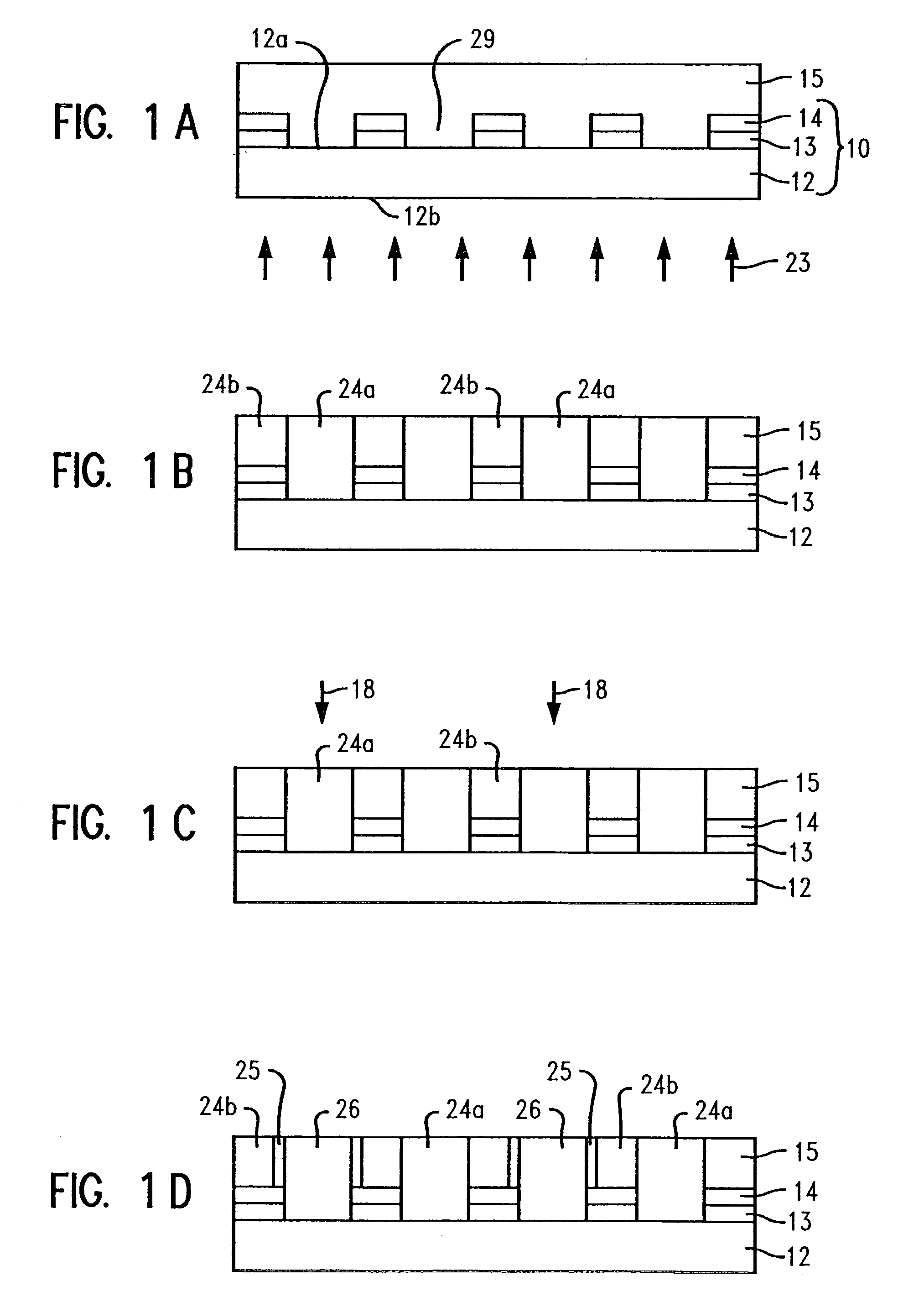
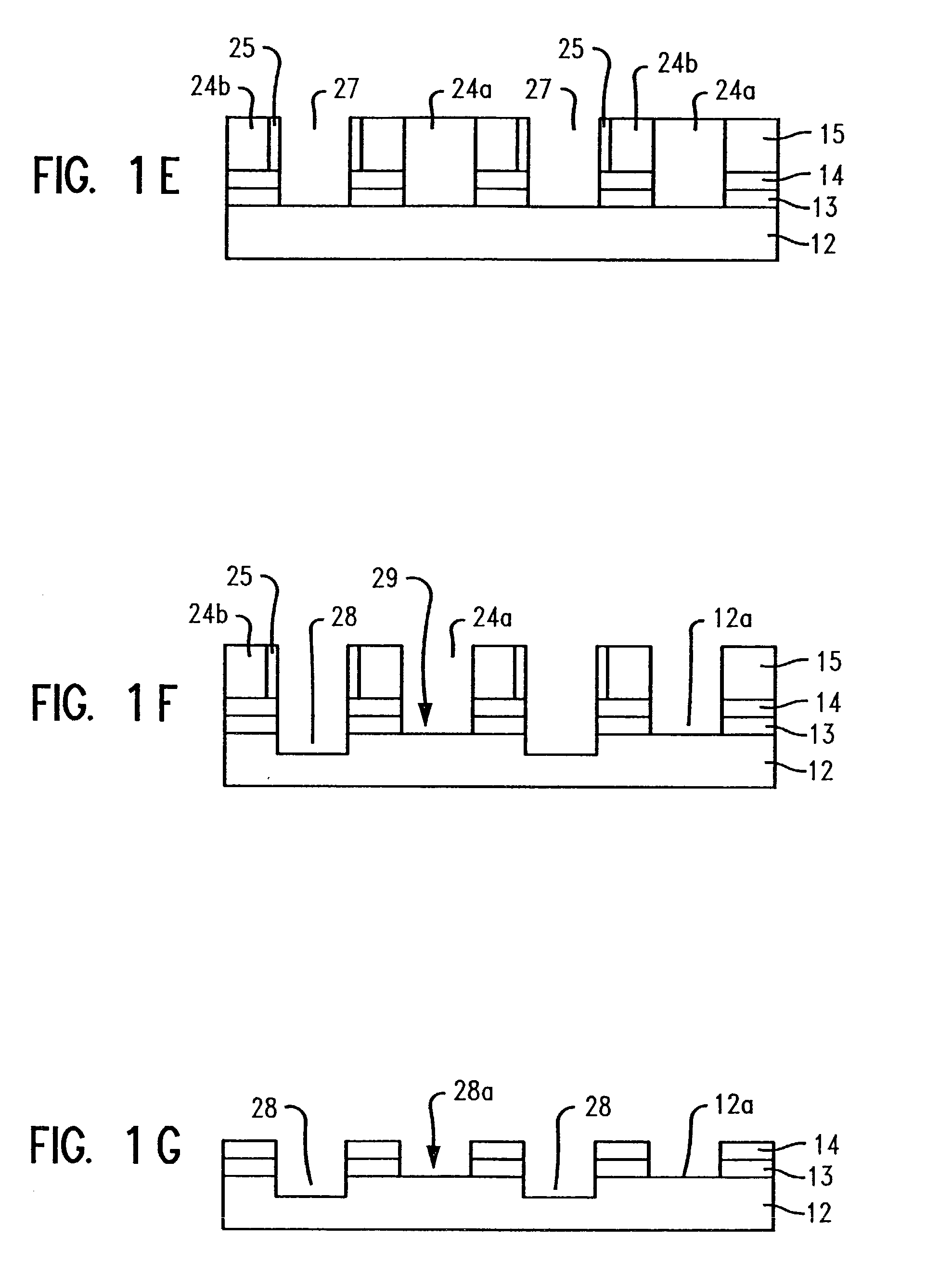
[0045] In describing the preferred embodiments of the present invention, reference will be made herein to FIGS. 1A-3 of the drawings in which like numerals refer to like features of the invention. Features of the invention are not necessarily shown to scale in the drawings.
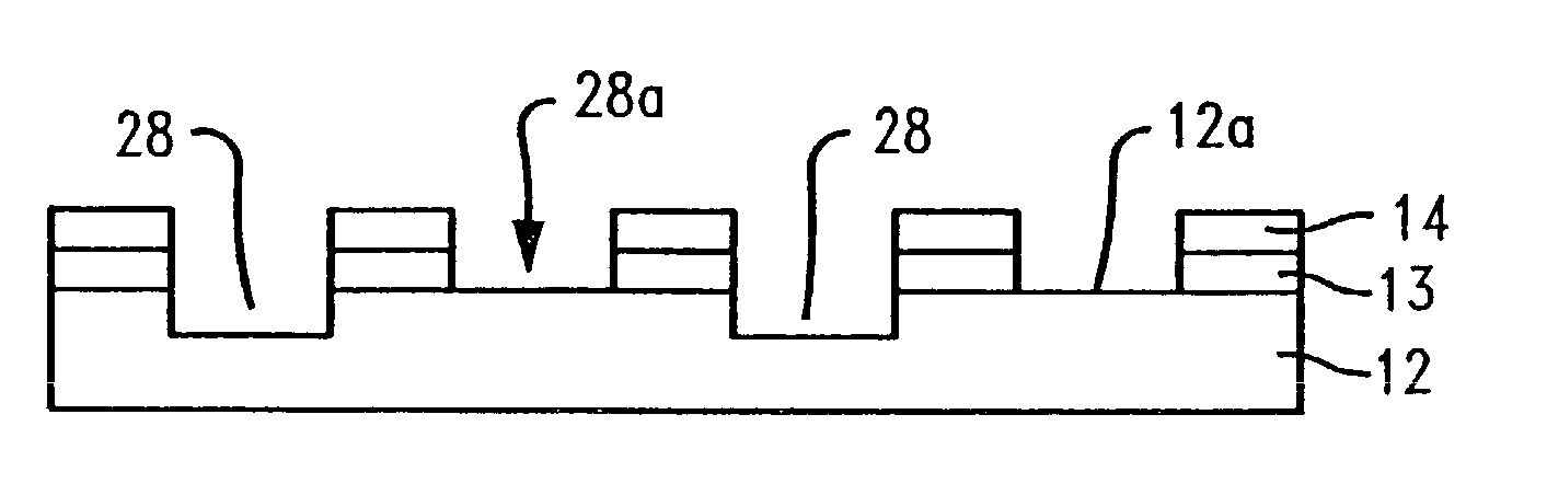
[0046] The present invention is directed to making phase shift masks, and, in particular, to making alternating phase shift masks, which masks contain an antireflective coating on the opaque design layer of the mask. The invention minimizes and / or avoids etching of the anti-reflective coating during the mask making method. For convenience, the following description will be directed to chrome-plated quartz or glass substrate photomasks which, as noted above, typically comprise a metal pattern such as chromium in a thickness of about 1000 .ANG. deposited on a transparent base such as glass or quartz.
[0047] The substrate of the mask is made from any material that will transmit electromagnetic radiation or other su...
PUM
 Abstract
Description
Claims
Application Information