Method of forming a thin film with a low hydrogen content on a semiconductor device

a technology of semiconductor devices and thin films, which is applied in the direction of coatings, chemical vapor deposition coatings, metallic material coating processes, etc., can solve the problems of high hydrogen content severely affecting the performance of semiconductor devices, and poor step coverage of lpcvd thin films

Active Publication Date: 2003-12-11
SAMSUNG ELECTRONICS CO LTD
View PDF12 Cites 102 Cited by
  • Summary
  • Abstract
  • Description
  • Claims
  • Application Information

AI Technical Summary

Problems solved by technology

The conventional deposition process, such as a low-pressure chemical vapor deposition (LPCVD) process, and plasma-enhanced chemical vapor deposition (PECVD) process are not suitable for forming a thin film on a state-of-the-art semiconductor device.
For example, a conventional CVD process deposits a thin film at a relatively high temperature, which severely influences a semiconductor device, e.g., the redistribution of dopants in the substrate.
A thin film deposited through the LPCVD process (LPCVD thin film) contains a high percentage of hydrogen and has poor step coverage.
On the other hand, a thin film deposited using a PECVD deposits a thin film at a relatively low temperature as compared with the LPCVD thin film, but it also has poor step coverage.
However, even though a SiN layer deposited using an ALD process has good step coverage and a low processing temperature, there is a problem with the dry and wet

Method used


Image

  • Method of forming a thin film with a low hydrogen content on a semiconductor device
  • Method of forming a thin film with a low hydrogen content on a semiconductor device
  • Method of forming a thin film with a low hydrogen content on a semiconductor device

Examples


embodiment 1

[0048] Embodiment 1

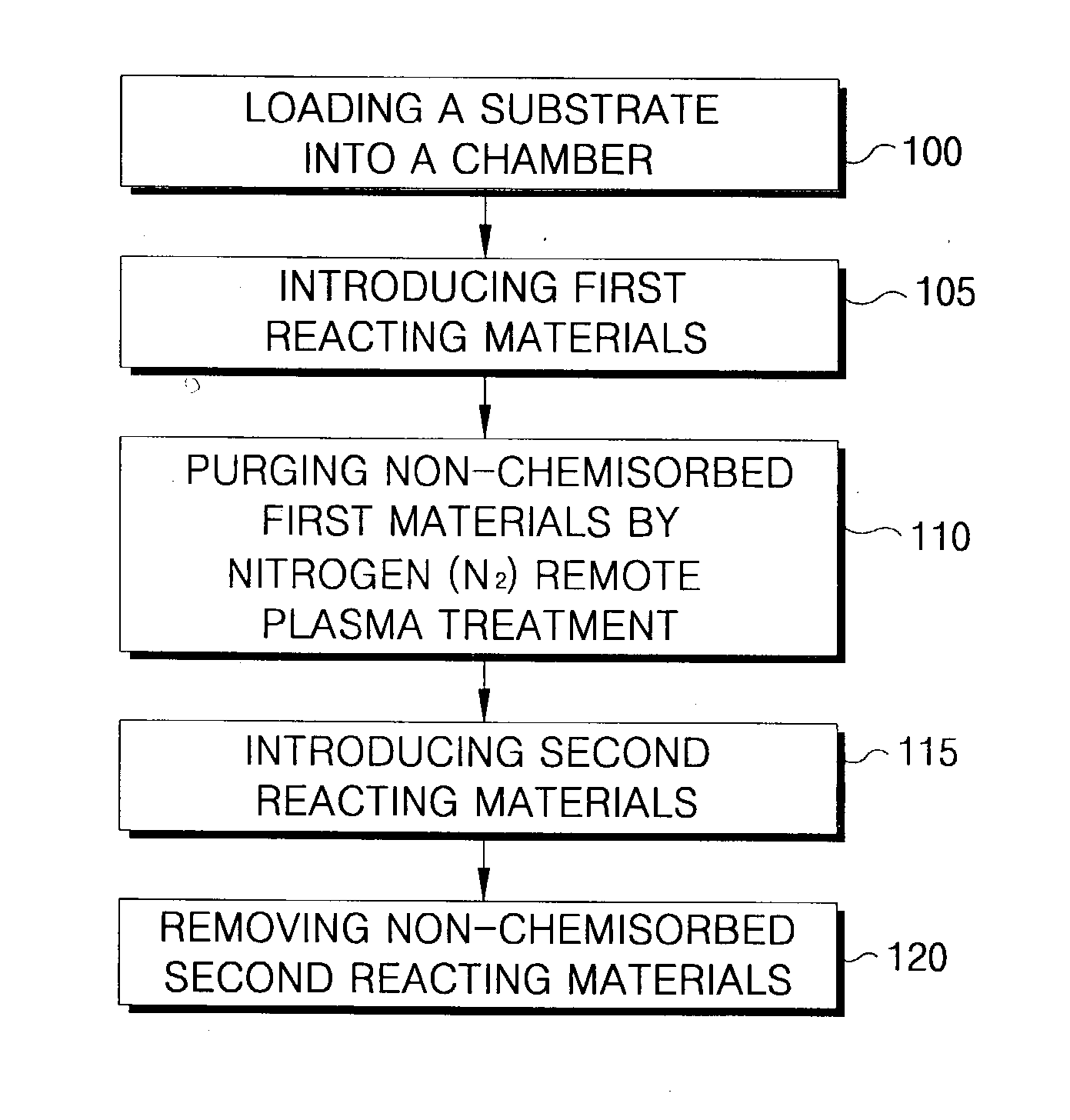
[0049] FIG. 4 is a flow chart explaining a method of forming a thin film according to a first embodiment of the present invention. Referring to FIG. 4, a method of forming a thin film according to the present embodiment is described as follows. Silicon nitride (SiN) is deposited using a ALD process, as described above, at a temperature of about 550.degree. C. The DCS gas and the ammonia (NH.sub.3) gas are used as the first and the second reacting materials, respectively. A flow rate of the ammonia (NH.sub.3) gas to the DCS gas is about 4.5:1. The ammonia (NH.sub.3) gas is provided by a remote plasma generator.

[0050] First, a silicon substrate is loaded into the chamber (step 100). A DCS dosing step is carried out for about 20 seconds so as to introduce the first reacting materials (step 105), and then the chamber is pumped out for about 10 seconds so that the internal pressure of the chamber is in a vacuum state. Next, the nitrogen (N.sub.2) gas, activated by the ...

embodiment 2

[0053] Embodiment 2

[0054] FIG. 5 is a flow chart explaining a method of forming a thin film according to a second embodiment of the present invention. Referring to FIG. 5, the method of forming a thin film according to the present embodiment is described as follows.

[0055] A silicon nitride (SiN) is deposited using an ALD process, as described above, at a temperature of about 550.degree. C. The DCS gas and the ammonia (NH.sub.3) gas are used as the first and the second reacting materials, respectively. A flow rate of the ammonia (NH.sub.3) gas to the DCS gas is about 4.5:1. The ammonia (NH.sub.3) gas is provided from remote plasma generator.

[0056] First, a silicon substrate is loaded into the chamber (step 200). A DCS dosing step is carried out for about 20 seconds to supply the first reacting materials in to the chamber (step 205), and then the non-chemisorbed DCS are purged from the chamber by supplying an inert gas, e.g., a nitrogen (N.sub.2) gas, into the chamber for about 3 seco...

embodiment 3

[0058] Embodiment 3

[0059] FIG. 6 is a flow chart for explaining a method of forming a thin film according to a third embodiment of the present invention.

[0060] According to this embodiment, a silicon nitride (SiN) is deposited using an ALD process, as described above, at a temperature of about 550.degree. C. The DCS gas and the ammonia (NH.sub.3) gas are used as the first and the second reacting materials, respectively. A flow rate of the ammonia (NH.sub.3) gas to the DCS gas is about 4.5:1. The ammonia (NH.sub.3) gas is provided by a remote plasma generator.

[0061] First, a silicon substrate is loaded into the chamber (step 300). A DCS dosing step is carried out for about 20 seconds to supply the first reacting materials into the chamber (step 305), and then the non-chemisorbed DCS is purged from the chamber by supplying an inert gas, e.g., as a nitrogen (N.sub.2) gas, into the chamber for about 3 seconds (step 310). After the chamber is purged of non-chemisorbed DCS, the chamber is...


PUM

PropertyMeasurementUnit
Concentrationaaaaaaaaaa
Contentaaaaaaaaaa

Abstract

A method of forming a thin film with a low hydrogen contents is provided by positioning a substrate inside a processing chamber, and supplying reacting materials into the chamber, chemisorbing a portion of the reacting materials onto the substrate. Then, a nitrogen (N2) remote plasma treatment is performed to reduce the hydrogen content of thin film layer formed by chemisorption of the reacting materials on the substrate. Accordingly, a thin film is formed having a low hydrogen content, since the hydrogen bonds in the thin film layer formed by chemisorption of the reacting materials are removed.

Description

[0001] 1. Technical Field Of The Invention[0002] The present invention generally relates to a method of forming a thin film on a semiconductor device; more particularly, a method of forming a thin film on a semiconductor device using an atomic layer deposition (ALD) process.[0003] 2. Discussion of the Related Art[0004] As semiconductor devices become more highly integrated, process conditions for forming a thin film on the semiconductor device, such as low heat budget, good step coverage, precise control for a thickness of the thin film, a low contaminated environment, etc., become more important.[0005] The conventional deposition process, such as a low-pressure chemical vapor deposition (LPCVD) process, and plasma-enhanced chemical vapor deposition (PECVD) process are not suitable for forming a thin film on a state-of-the-art semiconductor device. For example, a conventional CVD process deposits a thin film at a relatively high temperature, which severely influences a semiconductor...

Claims


Application Information

Patent Timeline
IPC IPC(8): C23C16/44C23C16/455C23C16/56H01L21/20H01L21/314H01L21/318
CPCC23C16/4554H01L21/3185C23C16/56C23C16/45546H01L21/02271H01L21/0228H01L21/0217H01L21/20H01L21/0234
Inventor LEE, SEUNG-HWANYANG, JONG-HO
Owner SAMSUNG ELECTRONICS CO LTD
Why Eureka
Try Eureka