Method of forming copper wiring in a semiconductor device

a technology of semiconductor devices and copper wires, applied in the direction of semiconductor devices, basic electric elements, electrical equipment, etc., can solve the problems of affecting the reliability of the device, the effect of improving the electrical characteristics and reliability of the devi

Active Publication Date: 2004-01-15
KEY FOUNDRY CO LTD
View PDF15 Cites 15 Cited by
  • Summary
  • Abstract
  • Description
  • Claims
  • Application Information

AI Technical Summary

Benefits of technology

0017] Accordingly, a method of forming copper wirings in semiconductor devices is disclosed that is capable of preventing a dishing phenomenon or an erosion phenomenon occurring on the surface of the copper wiring...

Problems solved by technology

Further, thin copper films can increase the signal transfer rate due to their low resistivity.
If the chemical mechanical polishing process is performed in this state, there is a problem that a "dishing" phenomenon or an "erosion" phenomenon may occur on the top surface of the copper wiring.
This p...

Method used


Image

  • Method of forming copper wiring in a semiconductor device
  • Method of forming copper wiring in a semiconductor device
  • Method of forming copper wiring in a semiconductor device

Examples


Embodiment Construction

[0025] Reference will now be made in detail to the preferred embodiments of, examples of which are illustrated in the accompanying drawings.

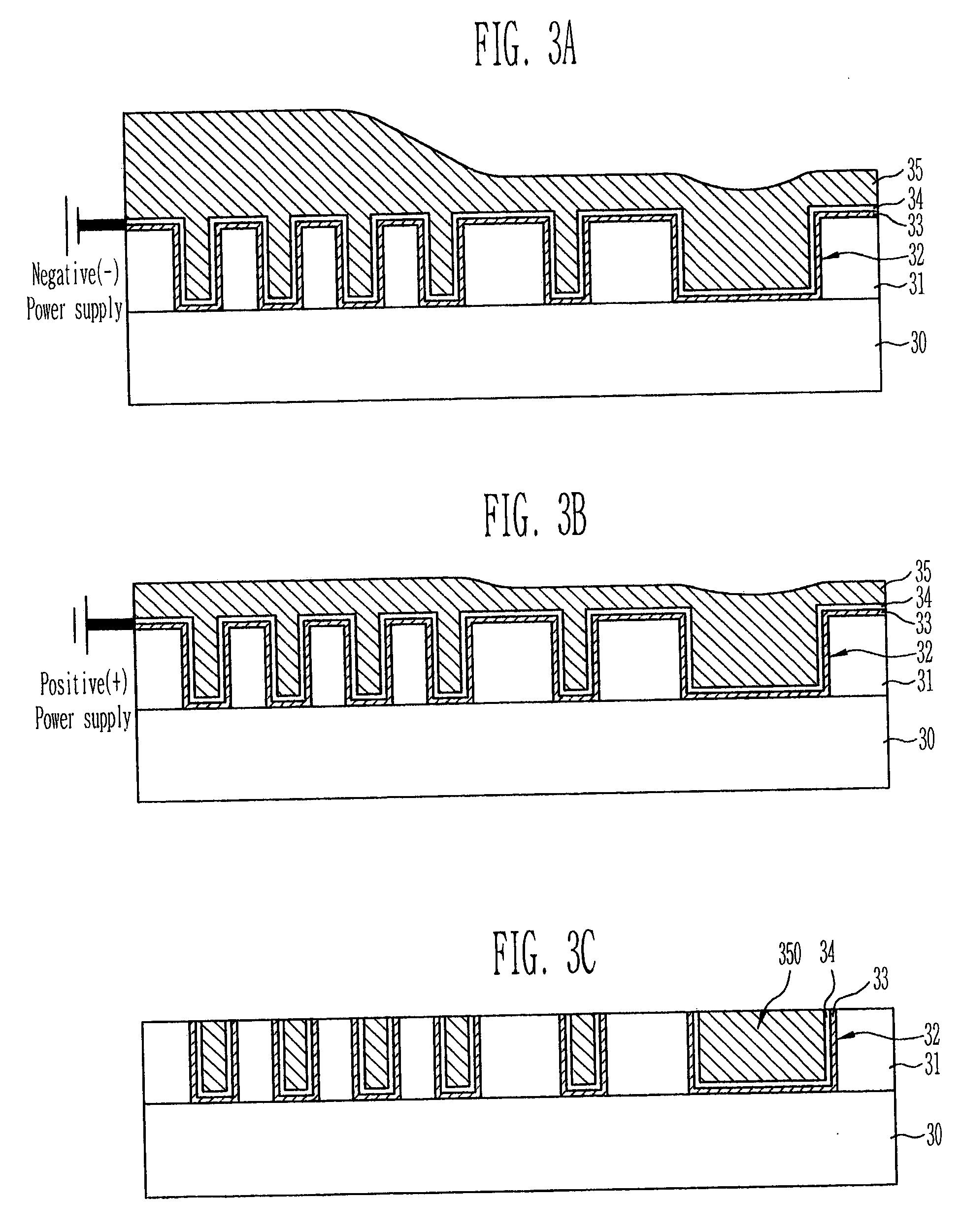
[0026] FIG. 3A through FIG. 3C are cross-sectional views of semiconductor devices for explaining a method of forming copper wirings in the device using an electroplating method according to a preferred embodiment.

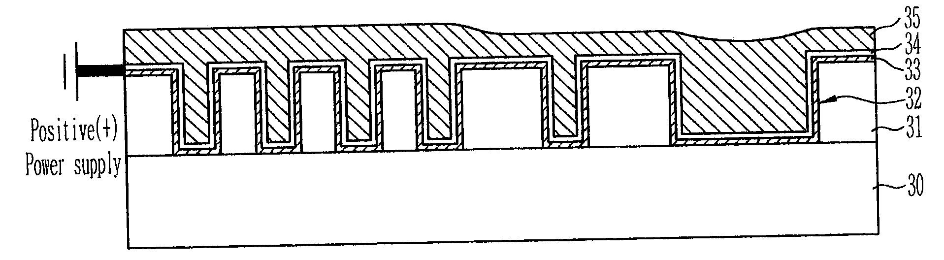
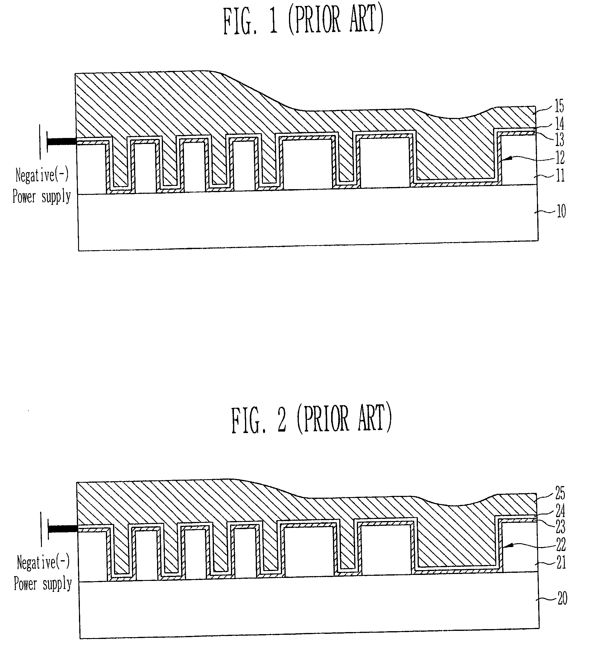
[0027] Referring now to FIG. 3A, an interlayer insulating film 11 is formed on a substrate 30. A plurality of damascene patterns 32 having different densities are then formed in the interlayer insulating film 31 by means of a damascene scheme. Next, a copper barrier metal layer 33 and a copper seed layer 34 are sequentially formed along the surface of the interlayer insulating film 31 including the plurality of the damascene patterns 32. Thereafter, a copper layer 35 is formed by means of a copper electroplating method so that the plurality of the damascene patterns 32 in which the copper seed layer 34 is formed are sufficiently filled....


PUM

PropertyMeasurementUnit
Thicknessaaaaaaaaaa
Electrical resistanceaaaaaaaaaa
Currentaaaaaaaaaa

Abstract

Disclosed is a method of forming a copper wiring in a semiconductor device. A copper barrier metal layer and a copper seed layer are sequentially formed along the surface of an interlayer insulating film including damascene patterns. In a state that a wafer is then loaded onto an electrical plating apparatus in which a copper plating solution is filled and a negative (-) power supply is also applied to the wafer, copper is plated so that the damascene patterns are sufficiently filled, thereby forming a copper layer. Next, the copper layer is polished in the plating solution by means of the electro-polishing process by changing the negative (-) power supply to the positive (+) power supply. Due to this, the surface of the copper layer is flat over the entire wafer. Thereafter, a chemical mechanical polishing process is performed until the surface of the interlayer insulating film is exposed, thereby forming copper wirings within the damascene patterns. As such, an uneven surface of the copper layer plated by the electroplating method is etched in the plating solution, thus making flat the surface of the copper layer and thin the thickness of the copper layer. It is thus possible to prevent a dishing phenomenon or an erosion phenomenon in a subsequent chemical mechanical polishing process. Therefore, the process margin of the chemical mechanical polishing process could be increased and process characteristics could be improved.

Description

[0001] 1. Technical Field[0002] A method of forming copper wiring in a semiconductor device is disclosed. More particularly, a method of forming copper wiring in a semiconductor device capable of preventing a dishing phenomenon or an erosion phenomenon occurring on the surface of the copper wiring when the copper wiring is formed in damascene patterns by polishing the copper layer using a chemical mechanical polishing (CMP) process.[0003] 2. Description of the Related Art[0004] In general, as the semiconductor industry shifts to ultra large-scale integration (ULSI), the geometry of semiconductor devices is narrowed to a sub-half-micron scale. The circuit density is increased improve performance and reliability. Thin copper films can improve reliability of the semiconductor device since they have a higher melting point than aluminum and thus have a higher resistance to electromigration (EM). Further, thin copper films can increase the signal transfer rate due to their low resistivity...

Claims


Application Information

Patent Timeline
IPC IPC(8): C25D5/18C25D7/12H01L21/28H01L21/288H01L21/321H01L21/768
CPCC25D5/18H01L21/2885C25D7/123H01L21/7684H01L21/76877H01L21/32115H01L21/28
Inventor KIM, SI BUM
Owner KEY FOUNDRY CO LTD
Why Eureka
Try Eureka