Nitride semiconductor light emitting diode

a light-emitting diode and semiconductor technology, applied in the direction of semiconductor devices, basic electric elements, electrical appliances, etc., can solve the problems of unsatisfactory directivity attained by this means, low and inability to perform satisfactorily increasing directivity. to achieve the effect of increasing the directivity of light-emitting diodes

Inactive Publication Date: 2004-01-29
TOYOTA CENT RES & DEV LAB INC
View PDF4 Cites 24 Cited by
  • Summary
  • Abstract
  • Description
  • Claims
  • Application Information

AI Technical Summary

Benefits of technology

0020] One aim of the present invention is to realize a technique for increasing the directivity of light projected from a nitride semiconductor light emitting diode.

Problems solved by technology

Since the main aim in conventional light emitting diodes is to ensure high visibility, these conventional light emitting diodes have low directivity of the projected light, and the projected light spreads across a wide area.
Although techniques of using a reflecting mirror or a lens to improve the directivity of the projected light are known, the directivity attained by this means remains unsatisfactory.
However, there has been no particular need to increase directivity in nitride semiconductor light emitting diodes, since these are mainly used for displays, and research that satisfactorily increases directivity has not been performed.
Further, it is difficult to obtain good quality crystal growth with nitride semiconductors that emit short wavelengths (blue light and green light) of visible light, therefore, nitride semiconductor lasers are not yet practical.
However, since the directivity thereof is low, light fails to enter the optical fibers, with the result that coupling efficiency with optical fibers is low.
However, if electric current first flows to areas in which the electric current flows most readily, the resistance in those areas drops, and a phenomenon is likely to occur whereby the electric current is concentrated in those areas.
One reason for this is that the directivity of the light projected from the conventional light emitting diode 120 is low, and so a large quantity of light leaks from the optical fiber.

Method used


Image

  • Nitride semiconductor light emitting diode
  • Nitride semiconductor light emitting diode
  • Nitride semiconductor light emitting diode

Examples


Embodiment Construction

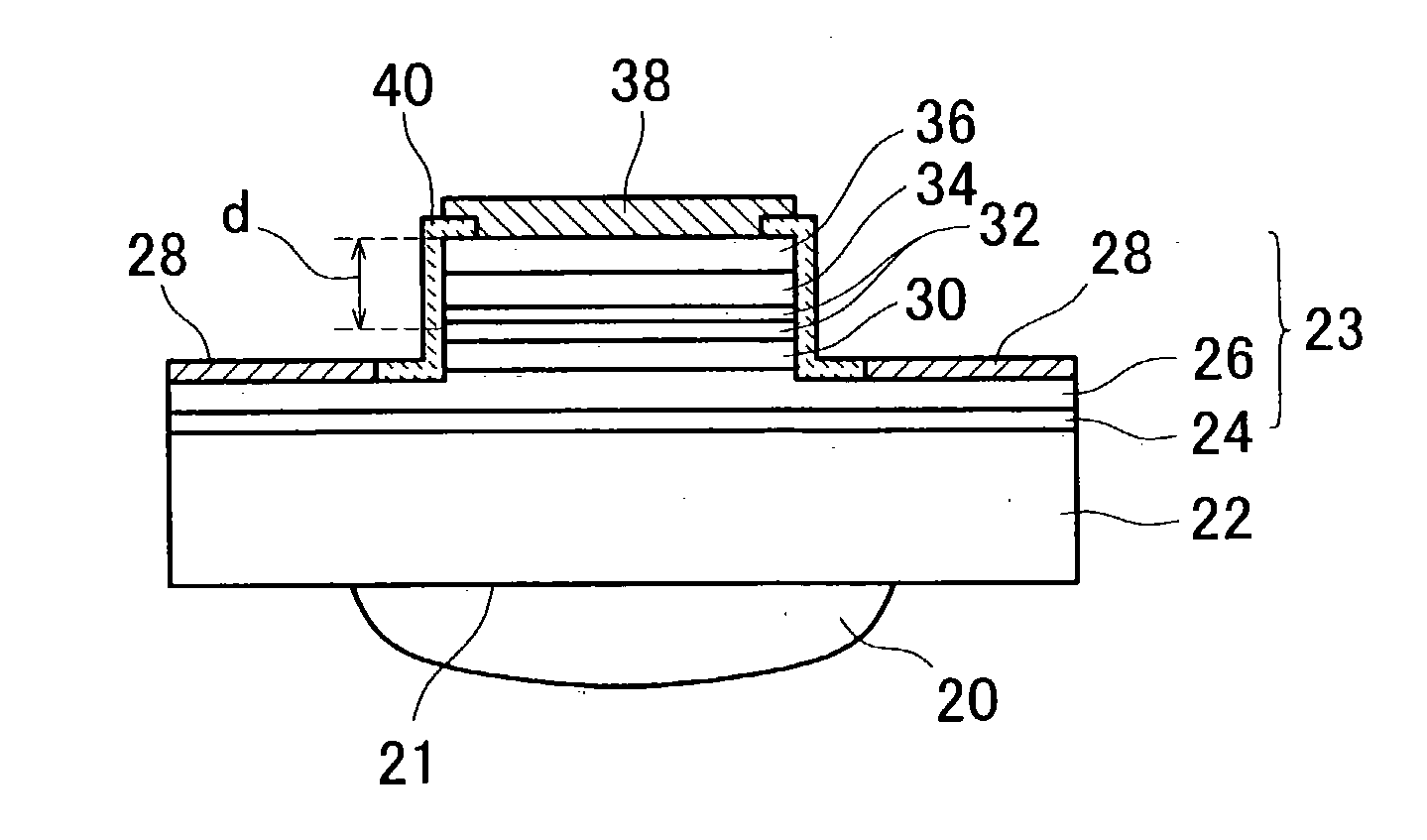
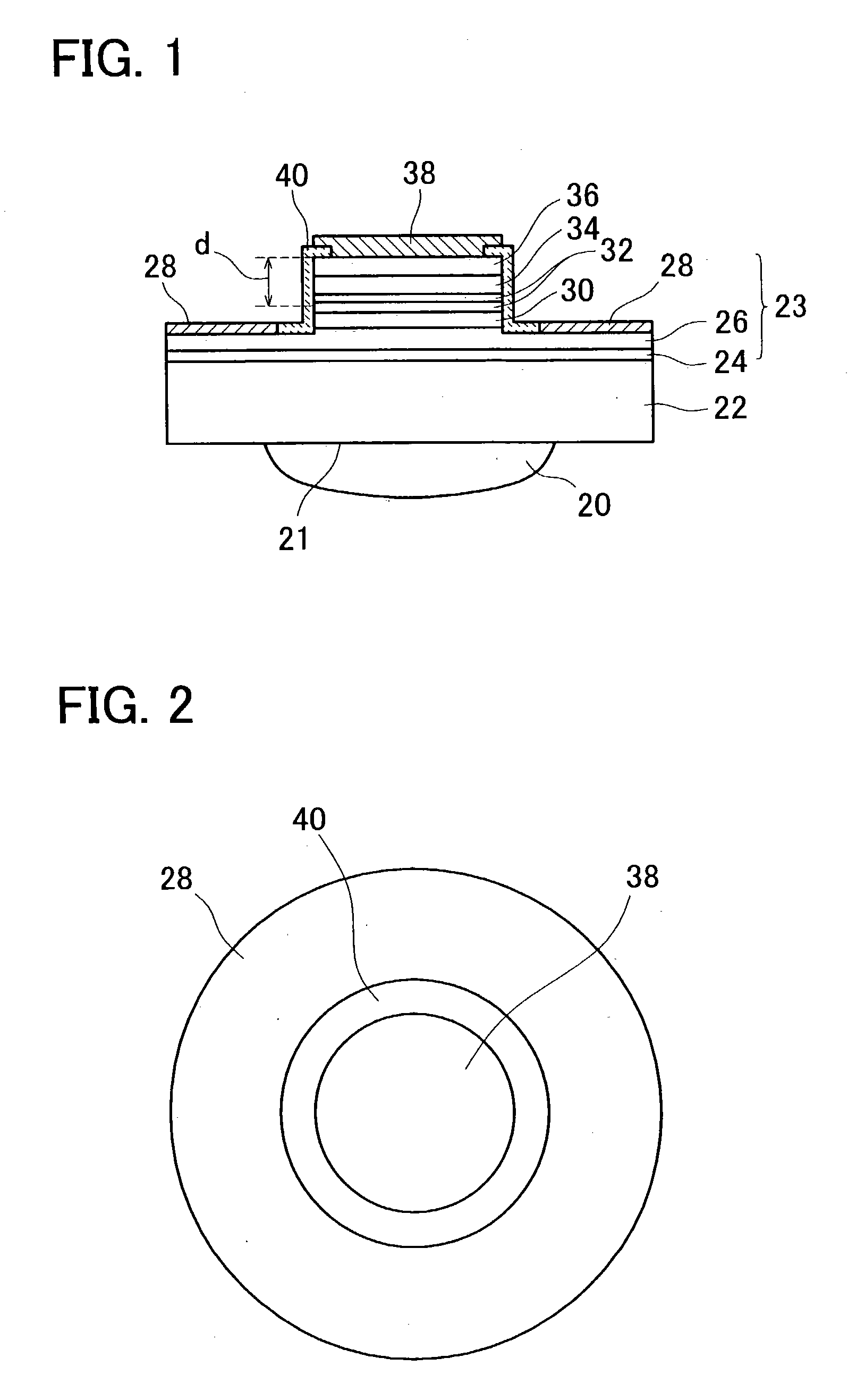
[0063] FIG. 1 is a schematic cross-sectional view showing a light emitting diode of an embodiment of the present invention, and FIG. 2 is a schematic plan view thereof. The light emitting diode is provided with a substrate 22, a layer structure 23, a p-electrode 38, an n-electrode 28, a silicon oxide film 40, and a lens 20. Laminated in the following sequence above the substrate 22 to form the layer structure 23 are: a buffer layer 24, an n-type contact layer 26, an n-type cladding layer 30, an active layer 32, a p-type cladding layer 34, and a p-type contact layer 36.

[0064] The substrate 22 may be formed from sapphire (Al.sub.2O.sub.3). Other material suitable for growing a nitride semiconductor, such as spinel (MgAl.sub.2O.sub.4), SiC, ZnO, GaN, etc. may be used as the substrate 22. The substrate 22 is transparent and is insulating. A back face of the substrate 22 is a light projecting face 21.

[0065] The buffer layer 24 may be formed from, for example, GaN, AIN, AlGaN, etc. The fi...


PUM


Abstract

An increased proportion of light projected from a nitride semiconductor light emitting diode enters the area within a specified angle. The nitride semiconductor light emitting diode is provided with an active layer 32 consisting of a nitride semiconductor, and a light projecting face 21. A reflecting mirror 38 is formed only on a side of the active layer 32 opposite the light projecting face 21. The reflecting mirror 38 is formed at a location from the center of the active layer 32 approximately (k.lambda/2+lambda/4)/n (where lambda is the wavelength of light projected from the active layer 32, n is the mean refractive index of an area between the active layer 32 and the reflecting mirror 38, and k is an integer). This light emitting diode allows directivity to be increased sufficiently, and the coupling efficiency thereof with optical fiber consisting of POF or the like can be improved.

Description

[0001] The present application claims priority on the Japanese Application No. 2002214322, filed Jul. 23, 2002.[0002] 1. Field of the Invention[0003] The present invention relates to a nitride semiconductor light emitting diode.[0004] 2. Related Art[0005] A nitride semiconductor light emitting diode (hereafter abbreviated to `light emitting diode`) having a nitride semiconductor active layer is known in the art. As shown in FIG. 22(A), light projected from an active layer 132 of a light emitting diode 120 forms a spherical wave spreading in all directions. The intensity distribution of the projected light is a function of the cosine of the angle .theta., as shown in FIG. 22(B). Directivity is not observed.[0006] Since conventional light emitting diodes are mainly used for displays, there is no particular need to improve the directivity of the projected light from the light emitting diodes. Instead, the main aim of the light emitting diode is to improve visibility.[0007] A light emit...

Claims


Application Information

Patent Timeline
Patent Type & Authority Applications(United States)
IPC IPC(8): H01L33/06H01L33/10H01L33/20H01L33/32H01L33/40H01L33/58
CPCH01L33/20H01L33/405H01L33/32
Inventor KACHI, TETSUKATO, SATORU
Owner TOYOTA CENT RES & DEV LAB INC
Why Eureka
Try Eureka