Semiconductor device and manufacturing method thereof

a technology of semiconductor devices and manufacturing methods, applied in semiconductor devices, semiconductor/solid-state device details, electrical apparatus, etc., can solve problems such as insufficient adhesion, insufficient affinitive, and inability to meet the requirements of affinitiveness

Inactive Publication Date: 2004-03-04
NEC ELECTRONICS CORP
View PDF5 Cites 21 Cited by
  • Summary
  • Abstract
  • Description
  • Claims
  • Application Information

AI Technical Summary

Problems solved by technology

However, a film constituted by a low dielectric constant insulating material is prone to cause imperfect adhesion with a film formed thereon or thereunder.
Especially when a porous material is employed as an insulating film, the problem of insufficient adhesion is significantly serious because of lower film density.
A probable reason of such phenomenon is that a methyl group contained in the MSQ layer is hydrophobic, and therefore not sufficiently affinitive with the SiCN.
However, since the SiCN layer 108 is also serving as a copper diffusion barrier constituting the copper interconnect line, a certain restriction is inevitably imposed when substituting a material.
The JP-A No.2001-326222 is not offering any solution of the imperfect adhesion at a lower interface of the MSQ layer.
Besides, the te

Method used


Image

  • Semiconductor device and manufacturing method thereof
  • Semiconductor device and manufacturing method thereof
  • Semiconductor device and manufacturing method thereof

Examples


Embodiment Construction

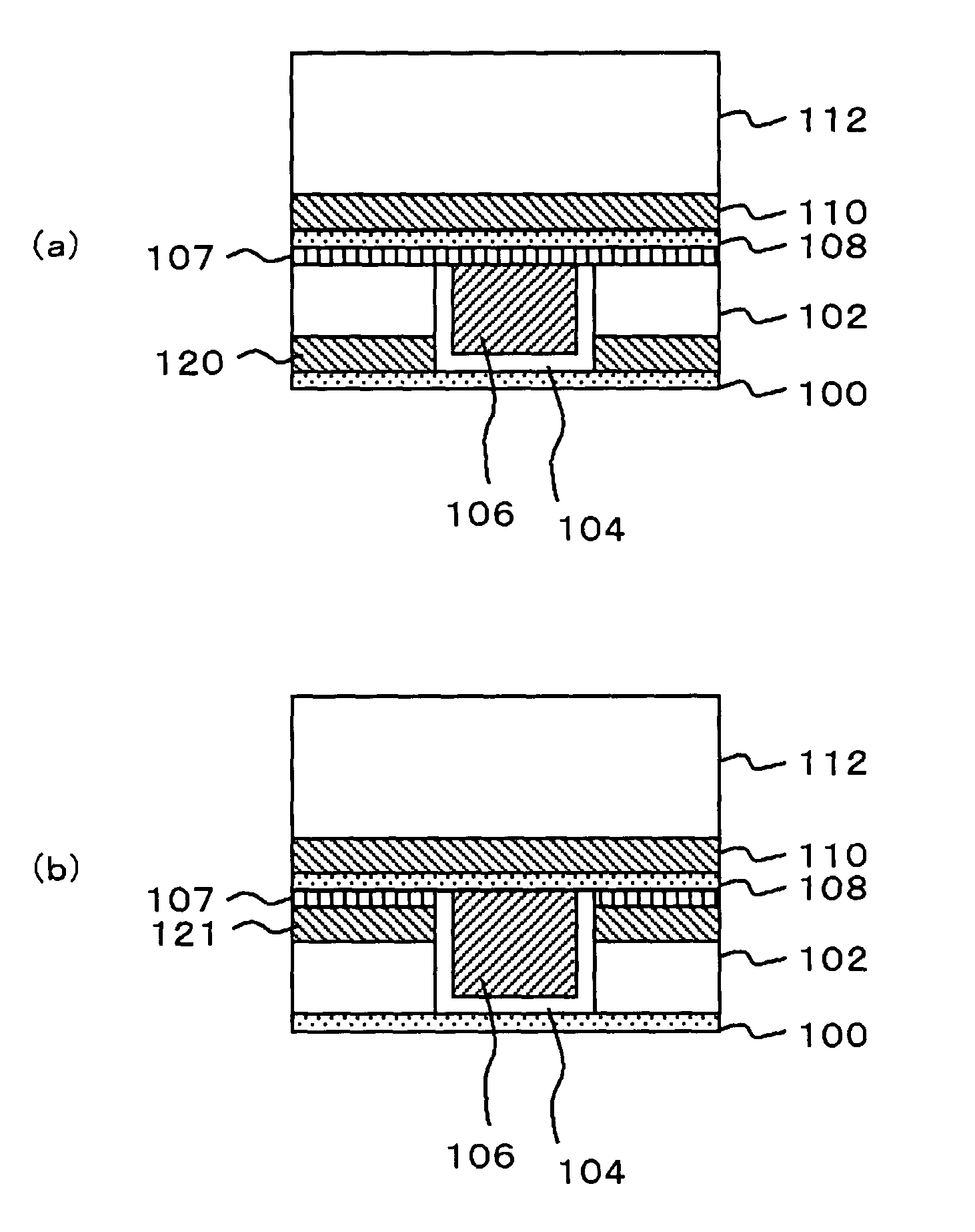
[0080] Adhesion between the MSQ layer and insulating layers adjacent the MSQ layer has been evaluated through a four-point bending test. FIG. 11A shows an illustration of how the sample to be tested was placed during the four-point bending test executed in the example. A sample was placed on a retainer having four supporting points. FIG. 11B is a schematic cross-sectional view of the sample. An MSQ layer 222, a silicon oxide layer 223, an epoxy layer 224 and a silicon layer 225 were laminated in this sequence on a substrate 221. A notch was introduced in a central portion of the silicon layer 225. When a load was imposed on the sample, a crack originating from the notch to a point on the substrate 221, from which point the crack further runs horizontally along an interface of the MSQ layer 222 and the substrate 221. Then, adhesion between the substrate 221 and the MSQ layer 222 was evaluated based on the load applied at this moment.

[0081] The substrate 221 was constructed such that ...


PUM


Abstract

An SiCN layer 108, BCB layer 110 and MSQ layer 112 are deposited in this sequence on a copper interconnect line constituted by a barrier metal layer 104 and a copper layer 106. The BCB layer 110 is formed by plasma polymerization of a monomer containing a divinylsiloxane bisbenzocyclobutene unit.

Description

[0001] This application is based on Japanese patent application NO.2002-255134, filed on Aug. 30, 2002, the content of which is incorporated hereinto by reference.[0002] 1. Field of the Invention[0003] The present invention relates to a technique for improving adhesion of an interlayer dielectric film utilizing a low dielectric constant insulating material.[0004] 2. Description of the Related Art[0005] Recently, as a semiconductor device has been increasingly required to operate at higher speed, various efforts are more intensely focused on the replacement of silicon oxide (dielectric constant K=approx. 4.3) making up an interlayer dielectric film with a material having a lower dielectric constant and then the reduction in parasitic capacitance between interconnect lines. HSQ, MSQ, and organic resin materials containing an aromatic compound, which have a dielectric constant of approx. 3, can be employed as the low dielectric constant insulating material, however for achieving a stil...

Claims


Application Information

Patent Timeline
IPC IPC(8): H01L21/312H01L21/768H01L23/522H01L23/532
CPCH01L21/3121H01L21/76801H01L21/76825H01L21/76826H01L21/76832H01L21/76834H01L21/76835H01L2924/0002H01L21/76849H01L23/522H01L23/53295H01L2924/00
Inventor OHNISHI, SADAYUKI
Owner NEC ELECTRONICS CORP
Why Eureka
Try Eureka