
Low dropout voltage regulator using a depletion pass transistor

a voltage regulator and depletion pass technology, applied in the field of electronic circuits, can solve the problems of system relatively insensitive to load, ldo oscillation, and architecture with severe performance limitations

Inactive Publication Date: 2004-03-11
DIALOG SEMICONDUCTOR GMBH
View PDF13 Cites 67 Cited by
  • Summary
  • Abstract
  • Description
  • Claims
  • Application Information

AI Technical Summary

Problems solved by technology

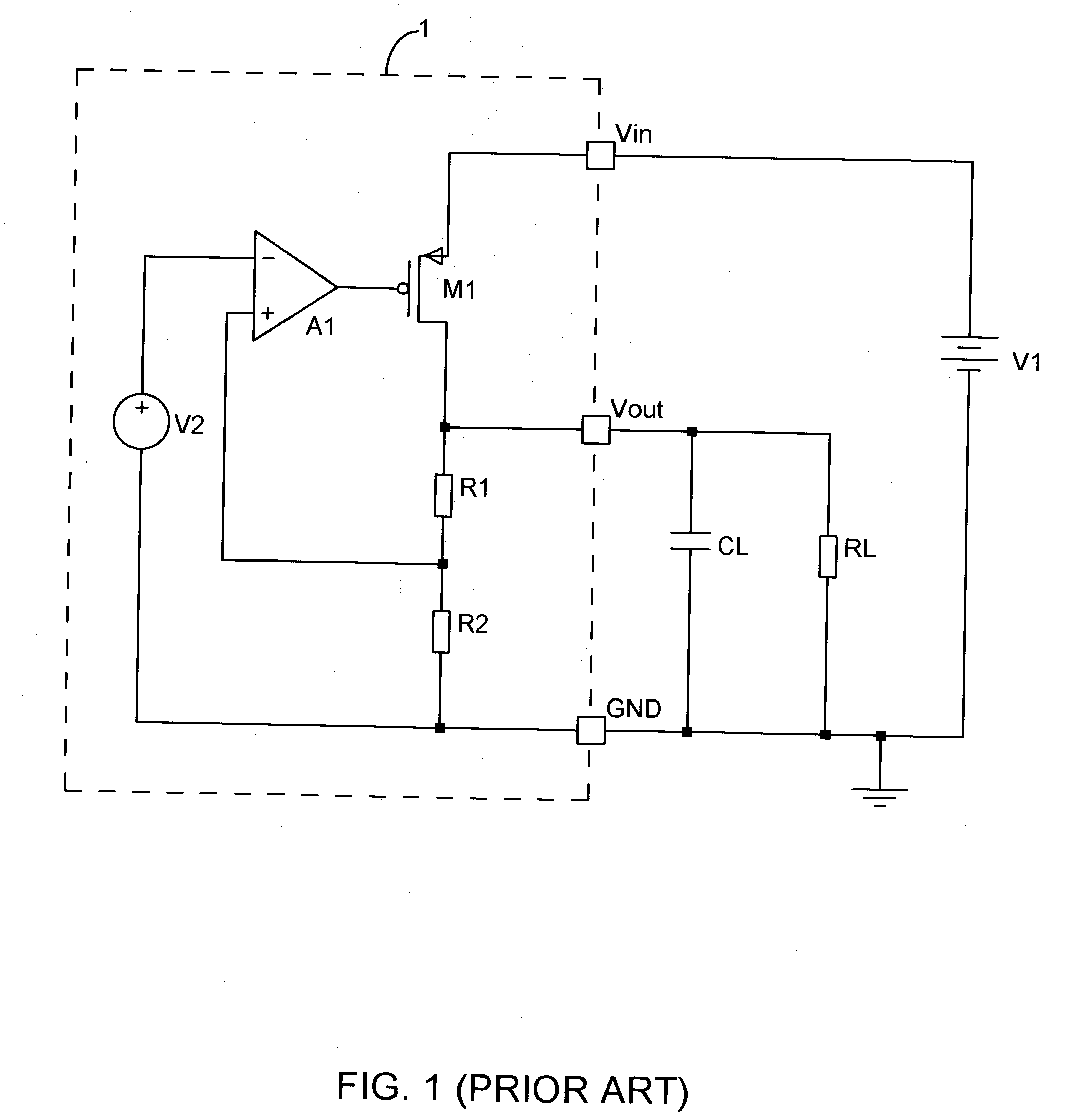
Although the low dropout of the standard LDO circuits is very desirable, this architecture has some severe limitations in performance.
Selecting the wrong capacitor (too large or too small, too much series resistance or too little) can cause the LDO to oscillate.
Because this architecture has inherently low output impedance, which is further lowered by feedback, the system is relatively insensitive to loading.
The reduction in feedback with increasing frequency can make the effective output impedance rise with frequency, causing it to look inductive.
This inductive output impedance can, under certain circumstances, interact with capacitive loading to reduce the stability of the system, but the systems are generally very wideband and load insensitive.
It is not possible to use existing commercial LDOs without a large capacitive load (equal to or exceeding 1 uF).
This results in the control loops of most LDOs being relatively slow.
Since the LDO has very high output impedance without feedback, and a relatively low gain at high frequencies, it cannot maintain its output voltage in the presence of fast load changes.
In all these cases the disadvantage is the need for an output capacitor to guarantee stability and adequate filtering of the output voltage.
There have been limited attempts to directly implement the older, faster control scheme in LDOs.
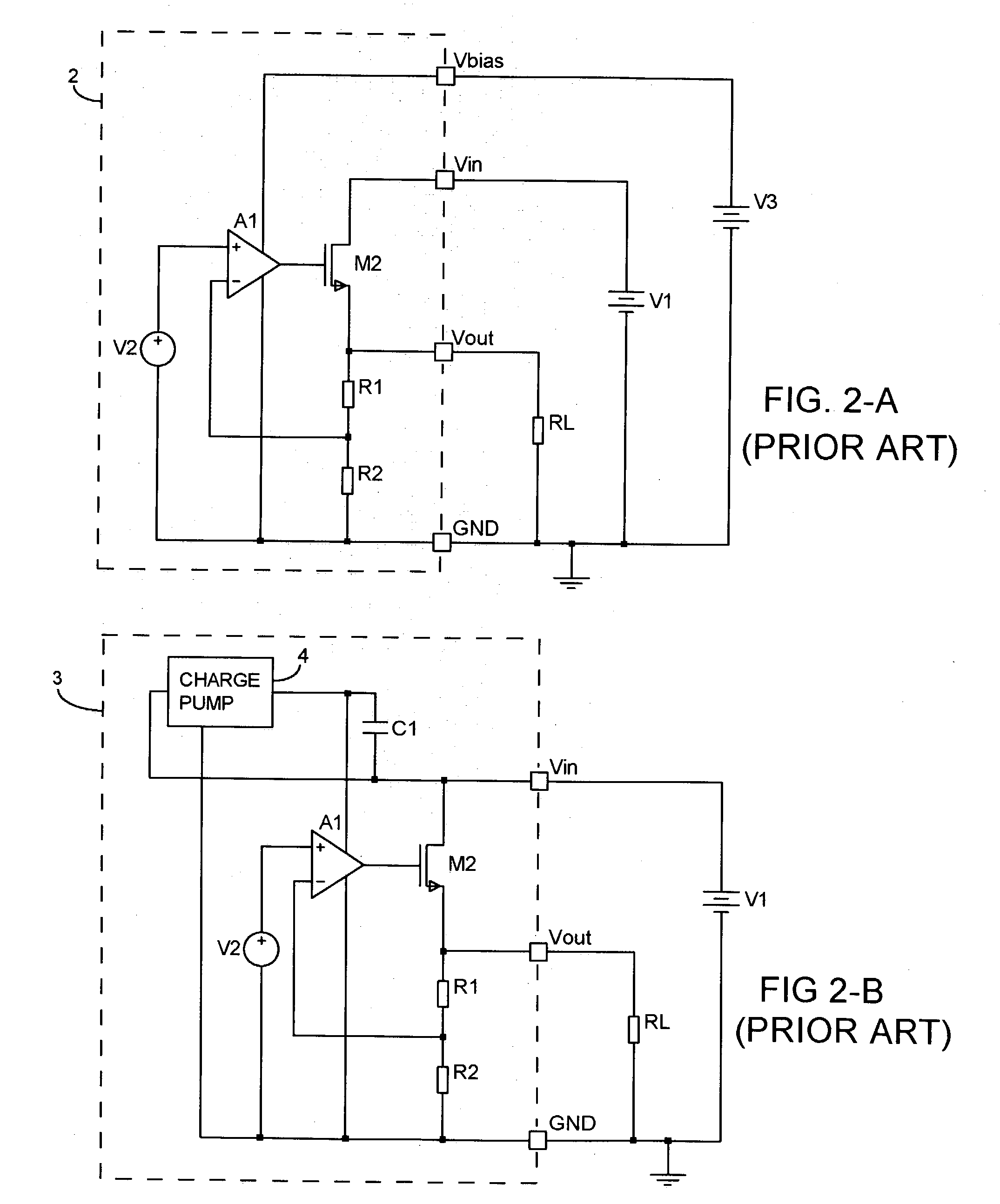
In principle, this second, higher voltage supply could be generated by the regulator 3 using a means such as a charge pump 4, as shown in FIG. 2B, but this would create unwanted noise and would delay startup until this required rail is generated.
But an additional selective implant into devices destined to be depletion FETs can easily alter the threshold such that it is negative, forming depletion devices.
There are several problems with the use of depletion mode pass devices, which are normally "on" and must have a negative voltage applied to their control terminal to turn them off.
One problem is that under a condition of shorted load, where the output is at ground potential, the device will be on and cannot be turned off without the application of a negative gate voltage.
Another potential problem with using depletion mode devices is that they are uncontrolled when voltage is initially applied.
This implementation is not the ideal configuration, because in the condition of very low dropout voltage, it is necessary to fully enhance both NMOS and PMOS devices, i.e. maximizing the voltage from gate to source.
When the regulated voltage is low, the PMOS device M3 in Wrathall cannot be fully enhanced.
If the off time is long enough, due to the natural current leakage present in any capacitor, the capacitor discharges itself, resulting in energy wasted at every cycle.
In the case of a shorted load, where the output terminal is at ground potential, it is not possible to drive the gate of the depletion device below ground to reduce the output current.

Method used


Image

  • Low dropout voltage regulator using a depletion pass transistor
  • Low dropout voltage regulator using a depletion pass transistor
  • Low dropout voltage regulator using a depletion pass transistor

Examples


Embodiment Construction

[0052] A. FIG. 5

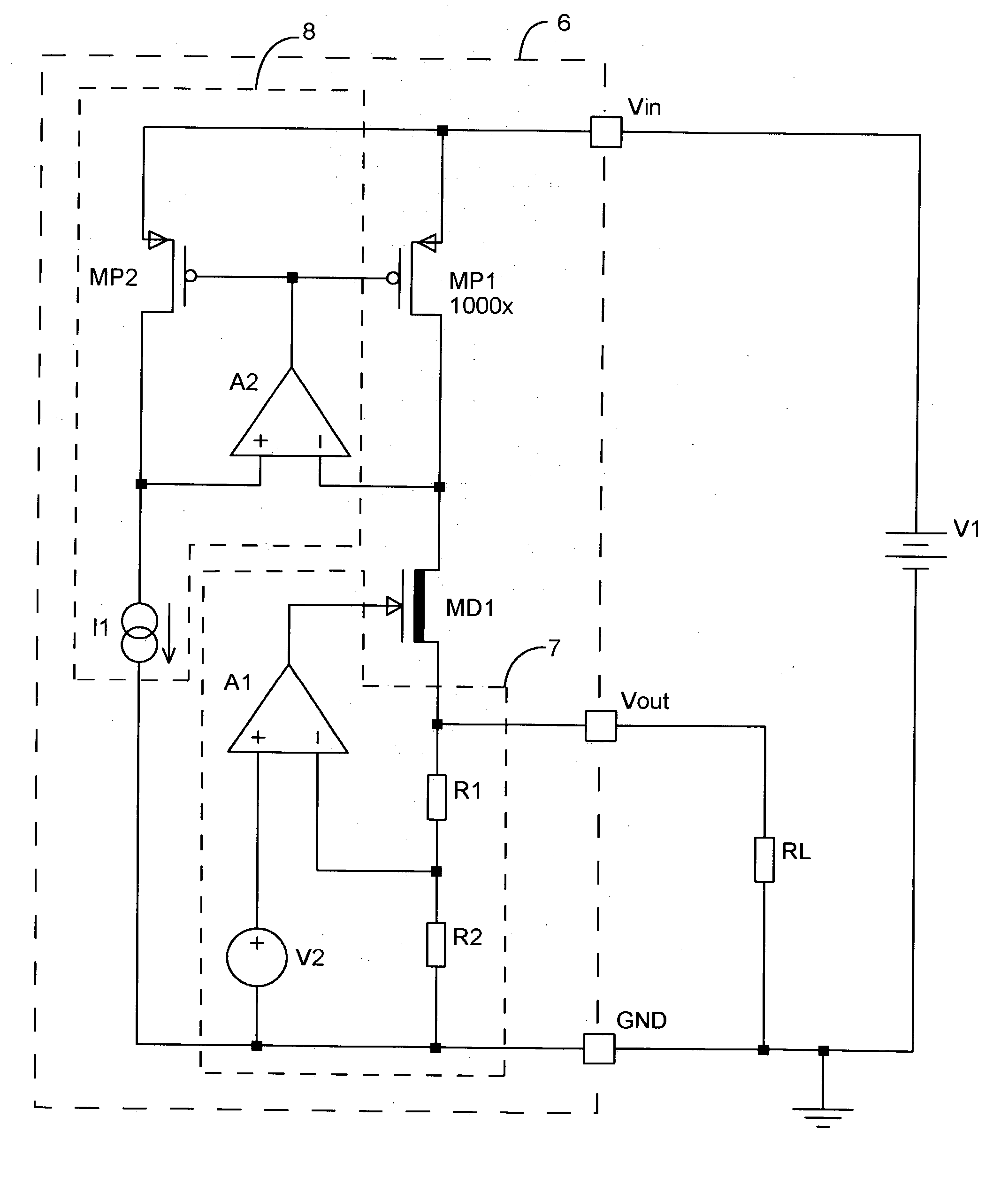
[0053] FIG. 5 shows the most general embodiment for the low dropout voltage regulator 6 using the depletion MOS transistor MP1 as main pass element.

[0054] The linear regulator 6 comprises a voltage control circuit 7 to control the voltage at the gate of the transistor MD1 in order to regulate the voltage at the load.

[0055] Furthermore a current control circuit 8 controls the voltage applied to the gate of PMOS device MP1 in order to control the current to the load.

[0056] According to the embodiment of the present invention, the depletion pass transistor MD1 is configured as a follower to allow the gate voltage to regulate the voltage at its source. Its back gate could be shorted to the source, but in a more common embodiment is connected to the substrate of the device. Because it is a depletion mode device, MD1 requires a negative voltage at its gate relative to its source in order to be turned fully off.

[0057] The PMOS device MP1 in series with pass device MD1 allow...


PUM


Abstract

A linear low dropout voltage regulator is described that makes use of a depletion mode NMOS pass transistor and of a PMOS transistor in series to the NMOS transistor and connected to its drain. The depletion NMOS transistor assures low dropout operations, while the series PMOS transistor allows the current regulation even under the condition of shorted load. The same PMOS transistor may be used to disable the current in the load without generating a negative voltage at the gate of the depletion pass transistor. This regulator is inherently stable without the need for an output capacitor in parallel to the load.

Description

RELATED APPLICATION DATA[0001] The present application claims priority from U.S. Provisional Patent Application No. 60 / 409,040 for LOW DROPOUT VOLTAGE REGULATOR USING A DEPLETION PASS TRANSISTOR filed on Sep. 9 2002.[0002] 1. Field of the Invention[0003] The present invention is in the field of electronic circuits. The present invention is further in the field of analog integrated circuits. The implementation is not limited to a specific technology (i.e. CMOS or bipolar), and applies to either the invention as an individual component or to inclusion of the present invention within larger systems which may be combined into a larger integrated circuit.[0004] The invention also falls within the field of DC voltage regulators and electronic power supplies, which convert energy from one DC level to another. These devices have been common in all electronic systems. More specifically, the invention falls into the class of voltage regulators referred to as series pass regulators or low drop...

Claims


Application Information

Patent Timeline
IPC IPC(8): G05F3/26
CPCG05F3/262
Inventor MENEGOLI, PAOLOSAWTELL, CARL K.
Owner DIALOG SEMICONDUCTOR GMBH
Learn More