Optical recording medium and method for recording and reproducing data
a technology of optical recording medium and data, which is applied in the direction of flat record carrier container, instruments, thermography, etc., can solve the problems of low storage reliability of optical recording medium, ag corrosion, and inability to reproduce data recorded in the l1 layer in a desired manner
- Summary
- Abstract
- Description
- Claims
- Application Information
AI Technical Summary
Benefits of technology
Problems solved by technology
Method used
Image
Examples
working example 1
[0128] An optical recording medium sample # 1 was fabricated in the following manner.
[0129] A disk-like polycarbonate substrate having a thickness of 1.1 mm and a diameter of 120 mm and formed with grooves and lands on the surface thereof was first fabricated by an injection molding process so that the track pitch (groove pitch) was equal to 0.32 .mu.m.
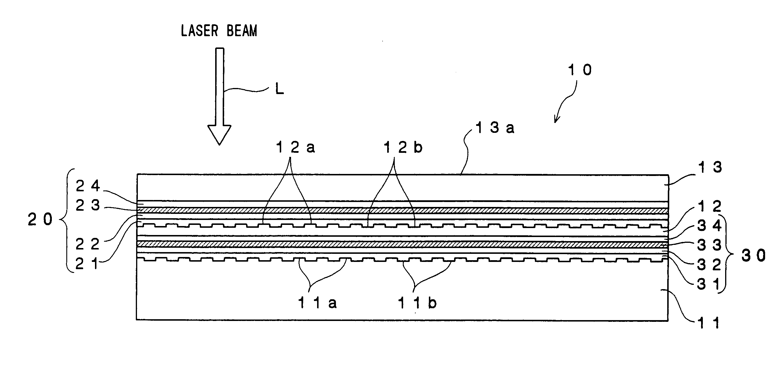
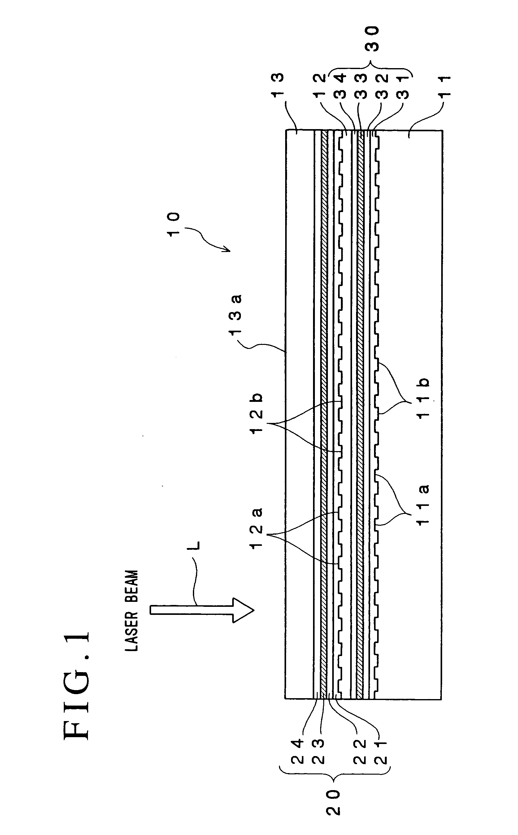
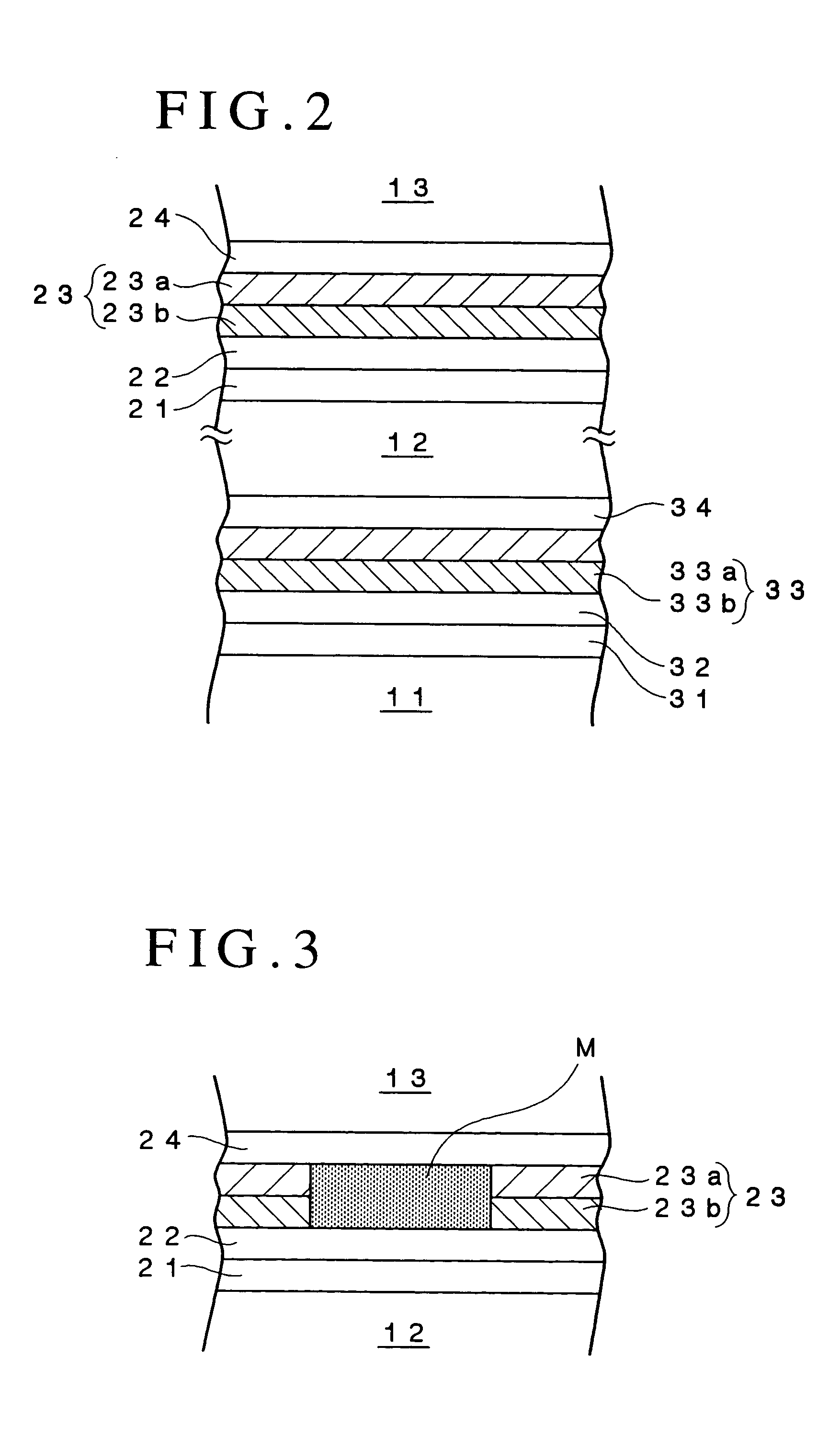
[0130] Then, the polycarbonate substrate was set on a sputtering apparatus and a reflective film consisting of an alloy of Ag, Pd and Cu and having a thickness of 100 nm, a fourth dielectric film containing a mixture of ZnS and SiO.sub.2 and having a thickness of 40 nm, a second L1 recording film containing Cu as a primary component and having a thickness of 3 nm, a first L1 recording film containing Si as a primary component and having a thickness of 3 nm and a third dielectric film containing the mixture of ZnS and SiO.sub.2 and having a thickness of 22 nm were sequentially formed on the surface of the polycarbonate substrate on whi...
working example 2
[0152] An optical recording medium sample # 4 was fabricated in the following manner.
[0153] A disk-like polycarbonate substrate having a thickness of 1.1 mm and a diameter of 120 mm and formed with grooves and lands on the surface thereof was first fabricated by an injection molding process so that the track pitch (groove pitch) was equal to 0.32 .mu.m.
[0154] Then, the polycarbonate substrate was set on a sputtering apparatus and a reflective film consisting of an alloy of Ag, Pd and Cu and having a thickness of 8 nm, a second dielectric film containing a mixture of ZnS and SiO.sub.2 and having a thickness of 28 nm, a second recording film containing Cu as a primary component and having a thickness of 5 nm, a first recording film containing Si as a primary component and having a thickness of 5 nm and a first dielectric film containing the mixture of ZnS and SiO.sub.2 and having a thickness of 22 nm were sequentially formed on the surface of the polycarbonate substrate on which the g...
PUM
| Property | Measurement | Unit |
|---|---|---|
| thickness | aaaaa | aaaaa |
| wavelength | aaaaa | aaaaa |
| light transmittance | aaaaa | aaaaa |
Abstract
Description
Claims
Application Information


