Heterojunction field effect transistor and manufacturing method thereof

a technology of field effect transistor and manufacturing method, which is applied in the direction of basic electric elements, electrical apparatus, and semiconductor devices, can solve the problems of deterioration of fet characteristics and fet characteristics, and achieve the effect of low deterioration of fet characteristics and high performan

Inactive Publication Date: 2004-04-29
PANASONIC CORP
View PDF13 Cites 20 Cited by
  • Summary
  • Abstract
  • Description
  • Claims
  • Application Information

AI Technical Summary

Benefits of technology

0007] The present invention has been proposed in view of the above problems. Accordingly, an object of the invention is to provide a high performance hetero

Problems solved by technology

Due to the annealing process, there arises such problem as the heterojunction is changed in nature resulting in a deterioration

Method used


Image

  • Heterojunction field effect transistor and manufacturing method thereof
  • Heterojunction field effect transistor and manufacturing method thereof
  • Heterojunction field effect transistor and manufacturing method thereof

Examples


first embodiment

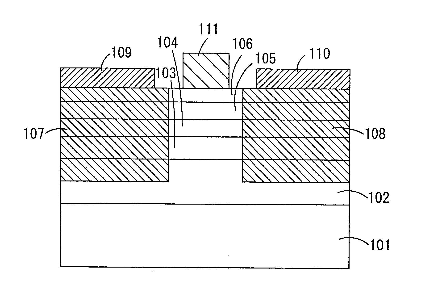
[0032] FIG. 1 is a cross sectional view showing a structure of a heterojunction FET according to the invention. In FIG. 1, formed on a semi-insulative GaAs substrate 101 are an undoped GaAs buffer layer 102, an undoped In.sub.0.2Ga.sub.0.8As layer 103 that serves as an active layer, an undoped Al.sub.0.2Ga.sub.0.8As layer 104 that serves as a spacer, an N-type Al.sub.0.2Ga.sub.0.8As layer 105 doped with Te, which serves as a carrier supply layer for supplying electron to the active layer, and an undoped GaAs layer 106. Reference numeral 107 denotes an N.sup.+-type source area formed of an Si ion implanted area, 108 denotes an N.sup.+-type drain area formed of an Si ion implanted area, 109 denotes a source electrode formed of a material from AuGe / Ni group, 110 denotes a drain electrode formed of a material from AuGe / Ni group, and 111 denotes a gate electrode formed of WSi / W.

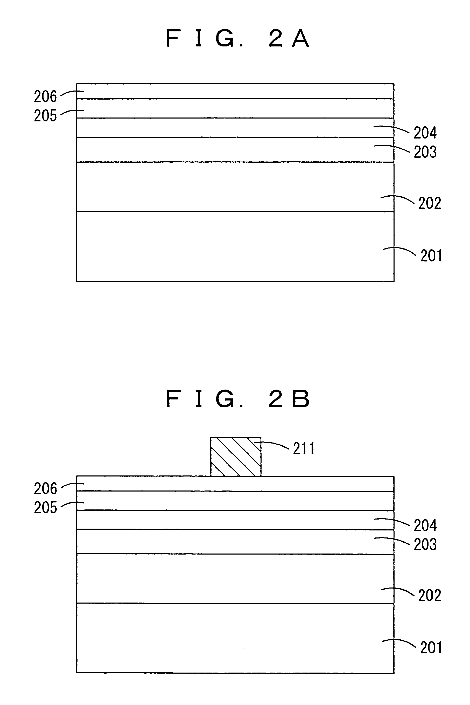
[0033] Next, referring to FIGS. 2A-2F, an example of manufacturing method of the heterojunction FET shown in FI...

second embodiment

[0043] FIG. 5 is a cross sectional view showing a structure of a heterojunction FET according to a second embodiment of the invention. In FIG. 5, formed on a semi-insulative GaAs substrate 501 are an undoped GaAs buffer layer 502, an N-type In.sub.0.2Ga.sub.0.8As layer 503 doped with Te that serves as an active layer, an undoped Al.sub.0.2Ga.sub.0.8As layer 504, and an undoped GaAs layer 505. Reference numeral 506 denotes an N.sup.+-type source area formed of an Si ion implanted area, 507 denotes an N.sup.+-type drain area formed of an Si ion implanted area, 508 denotes a source electrode formed of materials from AuGe / Ni group, 509 denotes a drain electrode formed of materials from AuGe / Ni group, and 510 denotes a gate electrode formed from WSi / W.

[0044] The second embodiment is different from the first embodiment in a point that the structure has no carrier supply layer, and the active layer is doped with Te.

[0045] The manufacturing method of the heterojunction FET according to the ...

third embodiment

[0047] FIG. 6 is a cross sectional view showing a structure of a heterojunction FET according to a third embodiment of the invention. In FIG. 6, formed on a semi-insulative GaAs substrate 601 are an undoped GaAs buffer layer 602, an In.sub.0.2Ga.sub.0.8As layer 603 that serves as an active layer, an undoped Al.sub.0.2Ga.sub.0.8As layer 604 that serves as a spacer, an N-type Al.sub.0.2Ga.sub.0.8As layer 605 doped with Se, which serves as a carrier supply layer for supplying electron to the active layer, and an undoped GaAs layer 606. Reference numeral 607 denotes an N.sup.+-type source area formed of a Si ion implanted area, 608 denotes an N.sup.+-type drain area formed of a Si ion implanted area, 609 denotes a source electrode formed of materials from AuGe / Ni group, 610 denotes a drain electrode formed of materials from AuGe / Ni group, and 611 denotes a gate electrode formed from WSi / W.

[0048] The structure according to the third embodiment is the structure of the first embodiment sho...


PUM


Abstract

In a heterojunction FET in which source and drain areas are formed by carrying out high temperature annealing process after carrying out ion implantation in areas to be formed into source and drain areas, conventionally, the N-type carrier supply layer and the N-type active layer are doped with Si. In place of doping with Si, doping with Se or Te is adopted. Thereby, in high temperature annealing process for activating the ion implanted areas, which serves as source and drain areas, unlike the Si donor, inactivation of donor due to reaction with F-atoms occurs scarcely with respect to the diffusion of F-atoms on the surface of the epitaxial substrate, which adhered during the process. Further, since the Se and Te are impurities from VI-family, when the Se or Te occupies any grid position of atoms from III-family or V-family, the Se or Te serves as the donor. Accordingly, a high performance heterojunction FET of little deterioration of the FET characteristics can be obtained.

Description

[0001] 1. Field of the Invention[0002] The present invention relates to a field effect transistor (hereinafter, referred to as FET) using a heterojunction epitaxial substrate and a manufacturing method thereof.[0003] 2. Description of the Related Art[0004] Since an FET of which source / drain area of a heterojunction FET is formed in a self-aligning manner with respect to the gate electrode using ion implantation has only a small parasitic resistance in the source / drain, it is expected as a process which realize a high performance enhancement type FET (for example, refer to "J. K. Abrokwah et al, GaAs IC Symposium Digest, P127-130, 1993").[0005] In the above heterojunction FET, for the carrier supply layer which supplies electron to the active layer, or for the active layer in which no carrier supply layer is provided but the active layer itself is doped, a layer doped with Si is mainly used.[0006] However, to activate an ion implanted area which serves as the source / drain area, a hig...

Claims


Application Information

Patent Timeline
IPC IPC(8): H01L29/812H01L21/338H01L29/207H01L29/778
CPCH01L29/7783H01L29/207
Inventor TAMURA, AKIYOSHIKOJIMA, KEISUKEKATO, YOSHIAKI
Owner PANASONIC CORP
Why Eureka
Try Eureka