Semiconductor device and method of producing the same

a semiconductor and semiconductor technology, applied in the direction of microstructural devices, microstructural technology, basic electric elements, etc., can solve the problems that the structure of wires, films, semiconductor elements formed on the main unit of the semiconductor substrate and/or the thin portion, or through the through hole, will be difficult to delaminate from the semiconductor device, and achieve excellent adhesiveness , the production process can therefore be simplified.

Inactive Publication Date: 2004-06-03
ROHM CO LTD
View PDF21 Cites 93 Cited by
  • Summary
  • Abstract
  • Description
  • Claims
  • Application Information

AI Technical Summary

Benefits of technology

0130] In this embodiment, the adhesiveness between the semiconductor substrate 2010 and the first organic film 2011 is inferior because the attachment is between an inorganic material and an organic material. However, no particular problems will occur between the first organic film 2011 and the semiconductor substrate 2010 so long as a force that is capable of delaminating the first organic film 2011 from the semiconductor substrate 2010 is not applied thereto. In addition, in situations in which through holes are formed in a portion of the first organic film 2011 and the inorganic film 2012 is directly adhered to the semiconductor substrate 2010, the attachment positions will have excellent adhesive

Problems solved by technology

Thus, structures such as wires, films, and semiconductor elements formed on the semiconductor substrate main unit

Method used


Image

  • Semiconductor device and method of producing the same
  • Semiconductor device and method of producing the same
  • Semiconductor device and method of producing the same

Examples


first embodiment

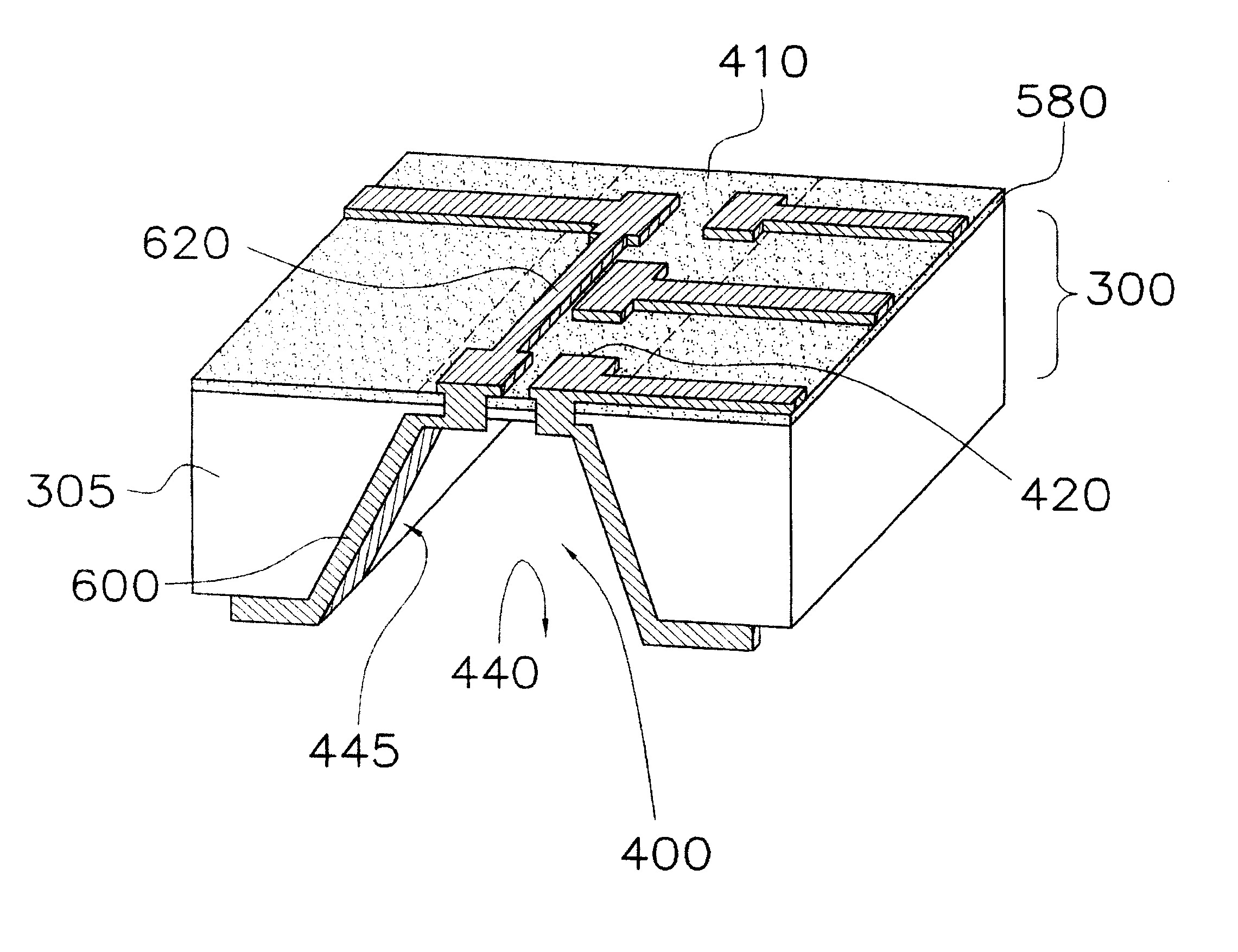
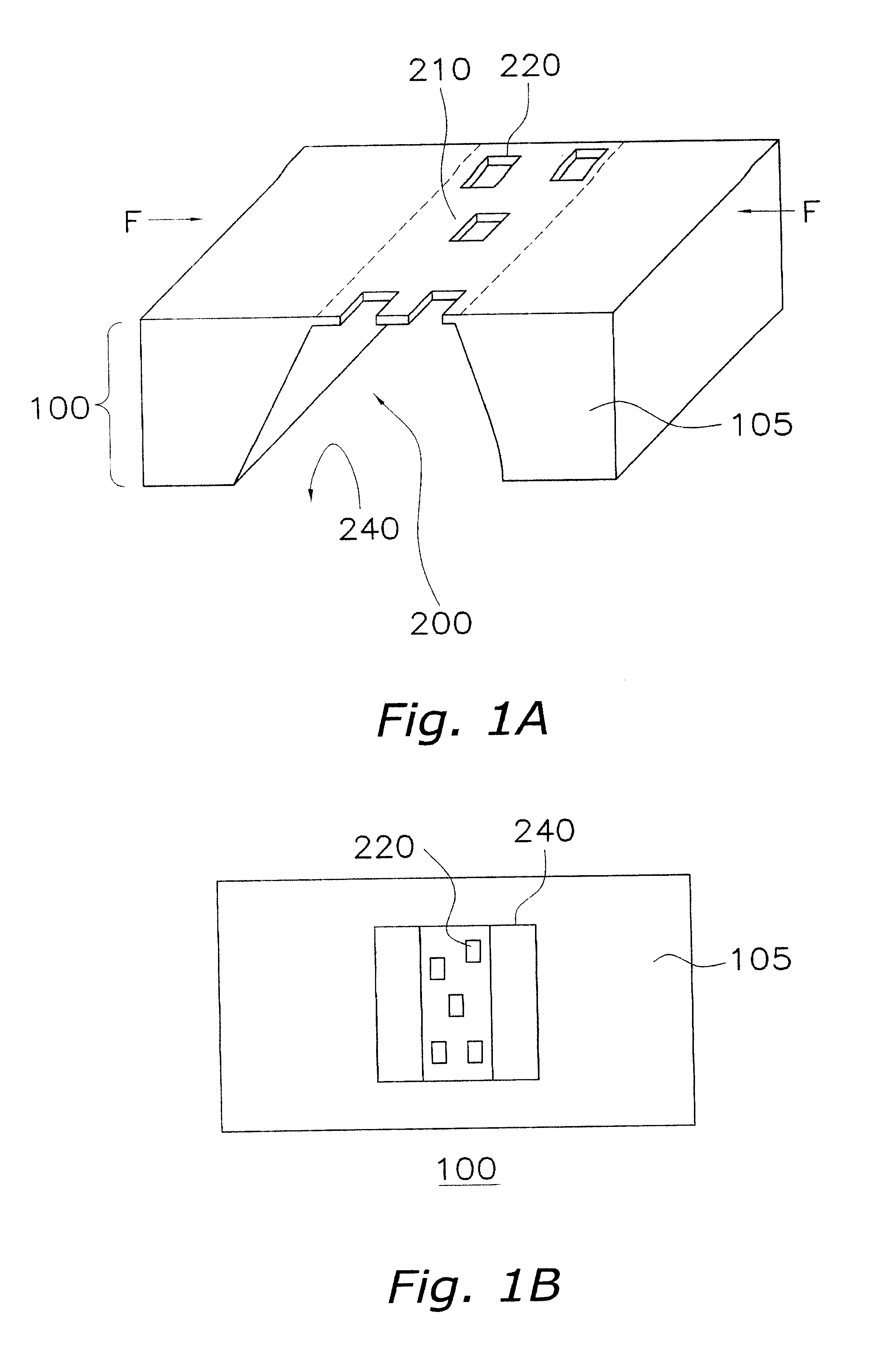
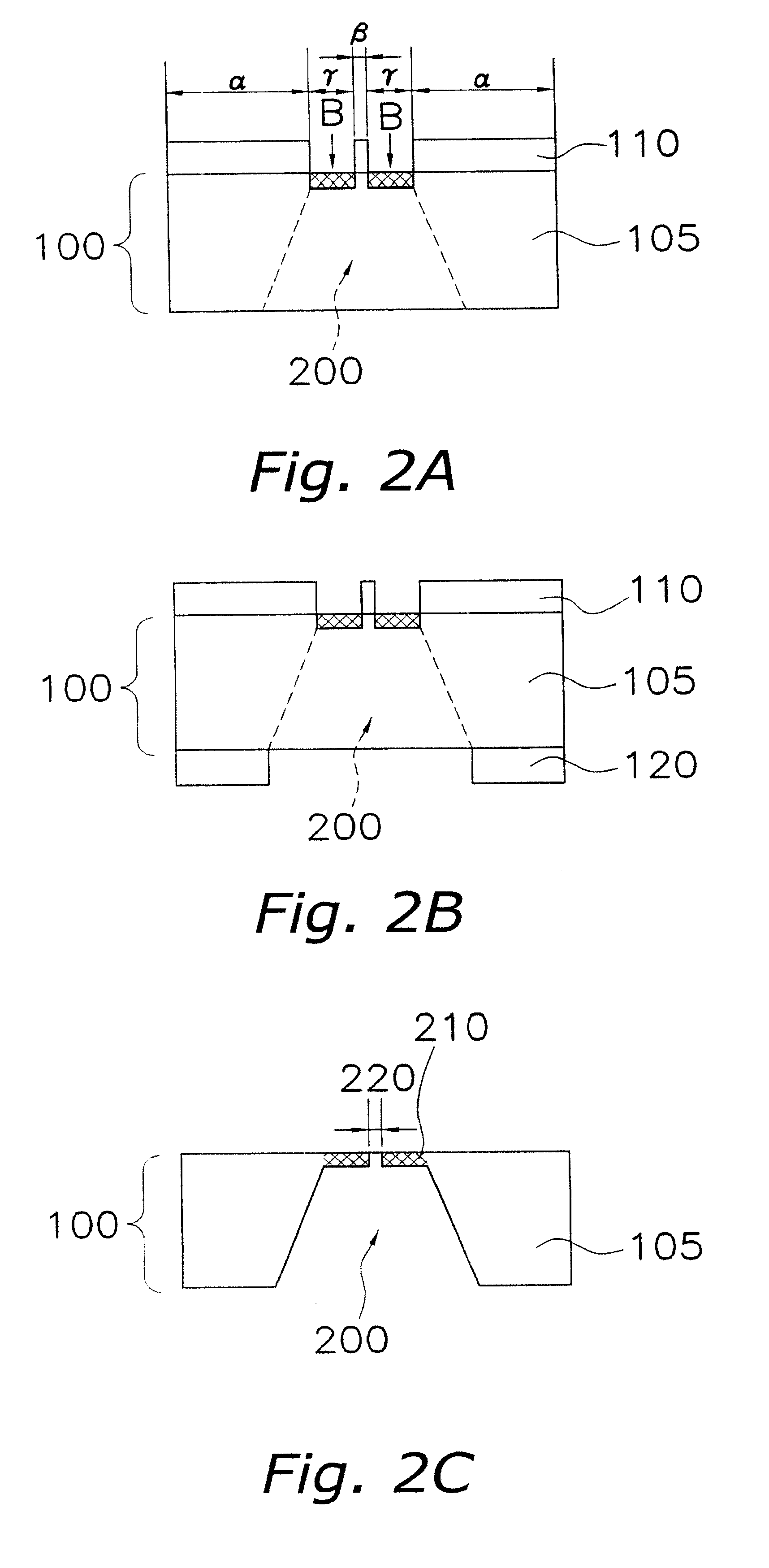
[0088] FIG. 7 is an example of the application of the basic structure of the first embodiment to a semiconductor device having microwiring. A semiconductor substrate 300 of this semiconductor device includes a semiconductor substrate main unit 305, a thin portion 410 on the upper surface side of the semiconductor substrate 300, an interlayer insulation film 580 formed on the semiconductor substrate 300, and wiring 600, 620. The thin portion 410 is positioned between the semiconductor substrate main unit 305, and is thinner than the semiconductor substrate main unit 305. Through holes 420 are formed in the thin portion 410. In addition, a recessed portion 400 and an opening 440 on the lower surface of the semiconductor substrate 300 are formed by means of the thin portion 410 and the semiconductor substrate main unit 305. The wiring 600 connects the upper surface and the lower surface of the semiconductor substrate 300, and is formed along a wall surface 445 of the recessed portion 4...

example 2

[0096] FIG. 9 is an example in which the semiconductor device of FIG. 7 is laminated. As shown in FIG. 9, a semiconductor element 500 that includes a gate electrode 520, a source 540, and a drain 560 is formed on a semiconductor substrate 350. The interlayer insulation film 580 and wiring 640, 645 are sequentially formed on the semiconductor element 500. The wiring 640, 645 are respectively connected to the source 540 and drain 560 via a contact hole in the interlayer insulation film 580. The semiconductor substrate 300 is laminated onto the upper portion of the semiconductor substrate 350 to form a unitary semiconductor device. The wiring structure on the upper portion of the semiconductor substrate 300 is identical to that shown in FIG. 7. Here, the electrical connection between the upper portion of the semiconductor substrate 300 and the lower portion of the semiconductor substrate 350 is carried out by connecting the wiring 640, 645 on the lower portion of the semiconductor subs...

example 3

[0097] FIG. 10 shows an example of a semiconductor device in which semiconductor elements are formed on the upper and lower surfaces of the semiconductor substrate. Semiconductor elements 900 that each include a gate electrode 920, a source 940 and a drain 960 are respectively formed on the upper and lower surfaces of a semiconductor substrate 700. An interlayer insulation film 980 and wiring 1000 are sequentially formed on each of the semiconductor elements 900. The semiconductor elements 900 on the upper and lower surfaces of the semiconductor substrate 700 are connected to each other by means of the wiring 1000. The wiring 1000 is formed on the thin portion 810 and the semiconductor substrate main unit 705, and is formed along a wall surface 845 of a recessed portion 800 via a through hole 820. Due to the above structure, the semiconductor device will be mechanically and structurally strengthened by the thin portion 810, and flexion of the semiconductor device will be reduced. As...


PUM


Abstract

A semiconductor device is disclosed which can be miniaturized and in which structures on a semiconductor substrate therein are difficult to delaminate, as well as a method of producing the same. The semiconductor device includes a semiconductor substrate main unit, and a thin portion that is thinner than the main unit and formed such that a recessed portion is formed in the semiconductor substrate and has at least one through hole formed therein. The thin portion is formed such that the etching rate of the thin portion is slower than the etching rate of the main unit. The thin portion provides a bridging structure between both sides of the recessed portion, and can mechanically and structurally strengthen the semiconductor device with respect to forces applied from the side surfaces of the main unit of the semiconductor substrate. Thus, structures such as wires, films, and semiconductor elements formed on the main unit and/or the thin portion of the semiconductor substrate or via the through holes will be difficult to detach from the semiconductor device.

Description

BACKGROUND OF INVENTION[0001] 1. Field of the Invention[0002] The present invention relates to a semiconductor device.[0003] 2. Background Information[0004] Micromachine technology has been proposed in the past that employs semiconductor materials such as silicon and the like. Devices that employ micromachine technology include sensors, semiconductor lasers, microactuators, fluid control devices such as micropumps and valves, and the like. With these types of devices, insulation film or metal patterns are generally used on the surface of the semiconductor substrate to form three dimensional structures. In addition, a metallic film (an inorganic film) is formed on the surface of the semiconductor substrate in a predetermined pattern, a resin film is then applied to the surface of the metallic film, and if the device is an ink jet head, a liquid chamber and ink flow paths that supply ink are then formed.[0005] FIG. 24A shows an oblique cross-sectional view of a conventional semiconduc...

Claims


Application Information

Patent Timeline
IPC IPC(8): B81B3/00H01L23/48H01L29/06
CPCB81B3/007B81B2201/052B81B2203/0315B81B2203/0353B81C2201/014B81C2201/019H01L2924/0002H01L23/481H01L29/0657H01L2924/12044H01L2924/00
Inventor TAKAOKA, MASAKISHIMOJI, NORIYUKI
Owner ROHM CO LTD
Why Eureka
Try Eureka