
Acoustic wave device and method of producing the same

a technology of acoustic wave and acoustic wave substrate, which is applied in the direction of semiconductor devices, basic electric elements, electrical apparatus, etc., can solve the problems of difficulty in forming a practical acoustic wave device directly on a semiconductor substrate, and the inability to integrate a conventional acoustic wave device with another electronic device,

Inactive Publication Date: 2004-06-03
FUJITSU MEDIA DEVICES +1
View PDF10 Cites 87 Cited by
  • Summary
  • Abstract
  • Description
  • Claims
  • Application Information

AI Technical Summary

Benefits of technology

[0020] A more specific object of the present invention is to provide an acoustic wave device that is hermitically sealed without an increase in size.
[0021] Another specific object of the present invention is to provide a method of producing a small and highly reliable acoustic wave device that can input and output electric signals without the use of metal wires or the likes.

Problems solved by technology

However, it is difficult to integrate a conventional acoustic wave device with another electronic device, not to mention the fact that a "system-on-chip" device cannot be achieved with the conventional acoustic wave device.
The first reason is the difficulty of forming a practical acoustic wave device directly on a semiconductor substrate.
From these facts, it is apparent that the use of acoustic wave devices has been a great hindrance to the production of smaller communication devices.
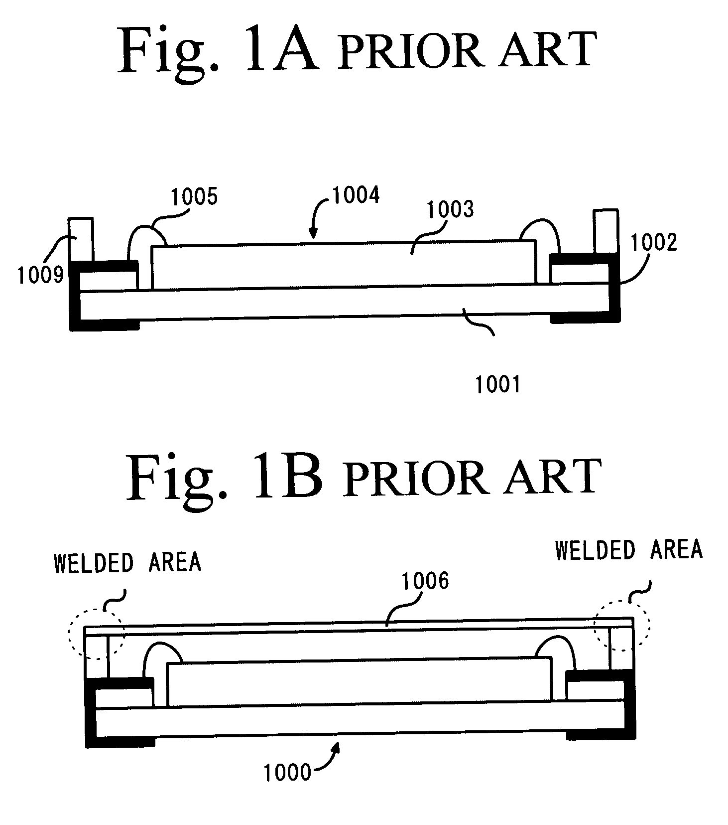
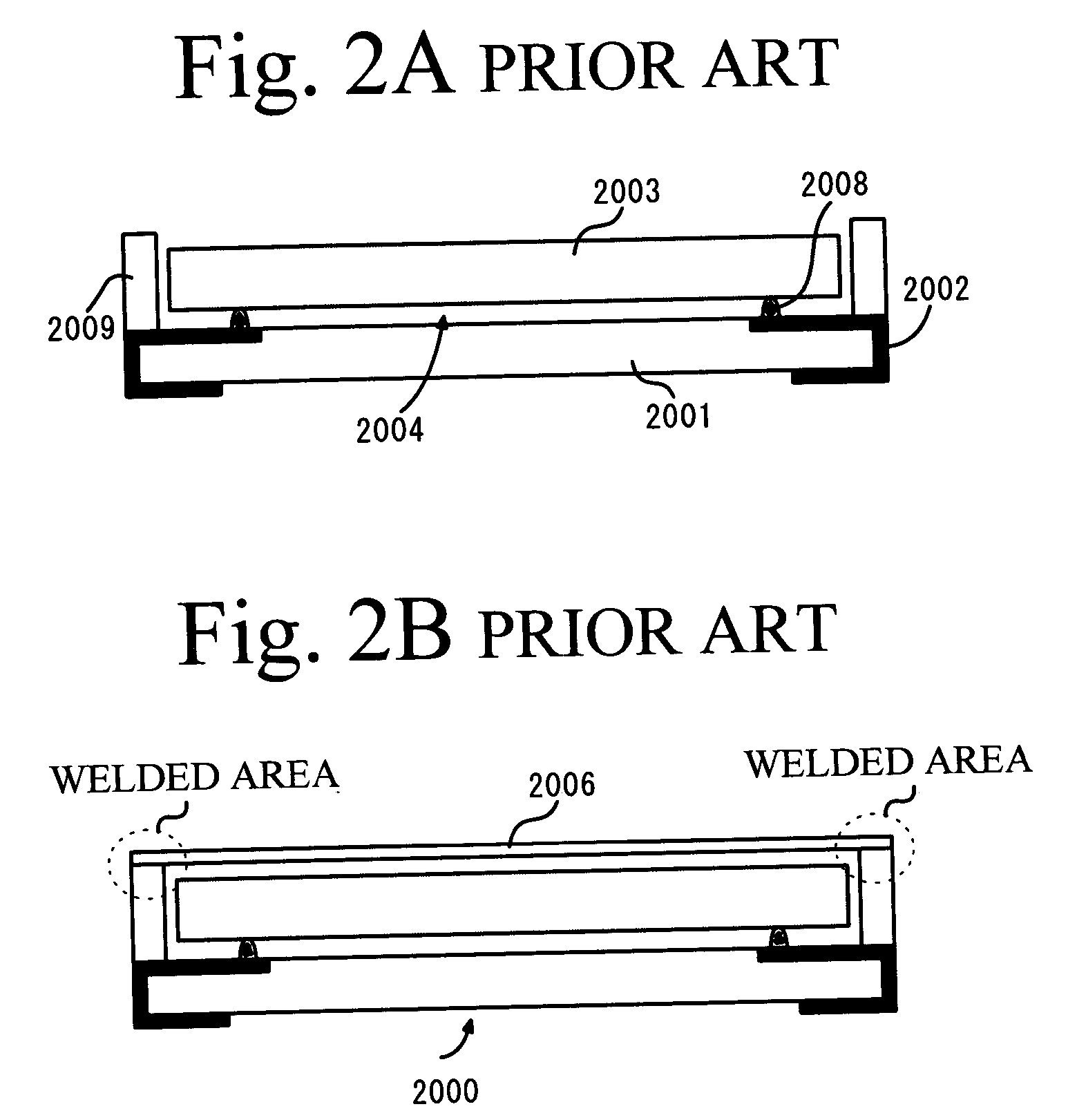
Although the package of the acoustic wave device can be made as small as the chip size in Prior Art 3, the mold made of plastic or resin cannot completely shut out the air (especially moisture).
This results in poor reliability in terms of moisture absorption.
Because of this, it is difficult to maintain sufficient reliability in a case where a module is formed by arranging the package and some other semiconductor chip on one substrate.
In such a case, it is necessary to employ an expensive hermetic seal for the entire module including the acoustic wave device.

Method used


Image

  • Acoustic wave device and method of producing the same
  • Acoustic wave device and method of producing the same
  • Acoustic wave device and method of producing the same

Examples


first embodiment

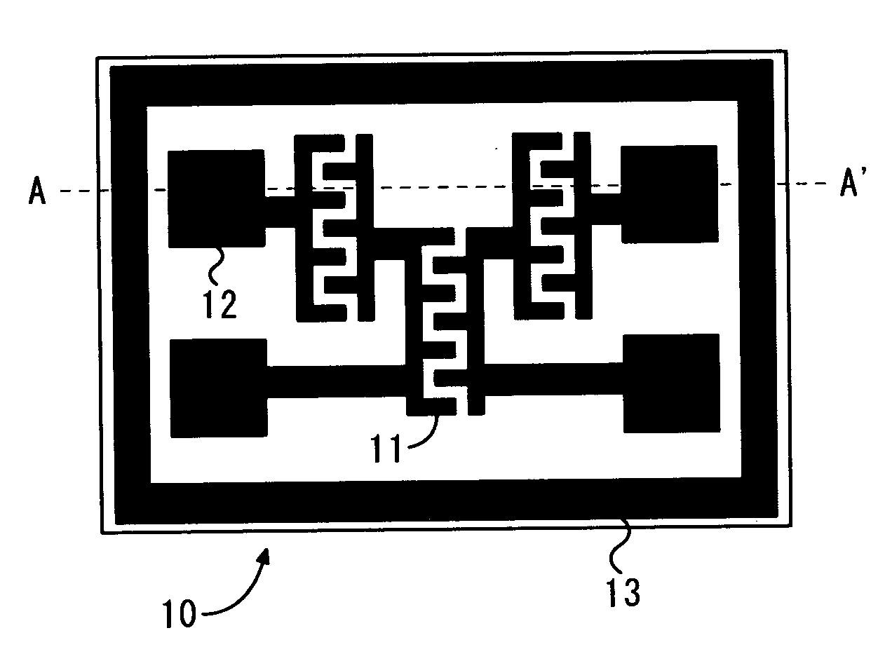
[0045] Referring to FIGS. 4A through 4C, the present invention will be first described. FIGS. 4A through 4C illustrate the structure of a chip 1 into which a surface acoustic wave device in accordance with this embodiment is incorporated. More specifically, FIG. 4A is a top view of a piezoelectric substrate 10 on which a comb-like electrode (IDT) pattern 11 is formed. FIG. 4B is a top view of a cover 20. FIG. 4C is a top view of the chip 1 formed by bonding the piezoelectric substrate 10 and the cover 20 to each other.

[0046] As shown in FIG. 4A, the IDT pattern 11, an electrode pad unit 12, and a peripheral metal layer 14, are formed on the piezoelectric substrate 10 that is produced by processing a semiconductor wafer. The IDT pattern 11 is part of a vibration unit that generates solid vibrations based on input electric signals. The electrode pad unit 12 electrically connects the IDT pattern 11 to the outside so as to introduce the electric signals. The peripheral metal layer 13 su...

second embodiment

[0062] Next, a second embodiment of the present invention will be described in detail, with reference to the accompanying drawings. This embodiment aims to simplify the structure and the production process through elimination of the hollow portion 22 of the cover 20 that is the second substrate. This embodiment also aims to increase the mechanical strength of the cover 20 and to reduce the production costs.

[0063] Referring now to FIGS. 6A through 7E, the structure of a chip 1A of this embodiment will be described in detail. FIGS. 6A through 6C illustrate the structure of the chip 1A. More specifically, FIG. 6A is a top view of a piezoelectric substrate 10A on which an IDT pattern 11 is formed. FIG. 6B is a top view of a cover 20A. FIG. 6C is a top view of the chip 1A formed by bonding the piezoelectric substrate 10A and the cover 20A to each other.

[0064] The piezoelectric substrate 10A shown in FIG. 6A has thin metal films 12A and 13A formed on an electrode pad unit 12 and a periphe...

third embodiment

[0074] Next, a third embodiment of the present invention will be described in detail, with reference to the accompanying drawings. In this embodiment, a bulk wave vibrator such as a crystal vibrator is employed, instead of the surface acoustic wave device of the first embodiment.

[0075] Referring to FIGS. 8A through 9D, the structure of a chip 2 of this embodiment will be described in detail. FIGS. 8A through 8D illustrate the structure of the chip 2. More specifically, FIG. 8A is a top view of an upper cover 51A that serves as the second substrate. FIG. 8B is a top view of a bulk wave vibrator 52 that serves as the first substrate. FIG. 8C is a top view of a lower cover 51B that serves as the third substrate. FIG. 8D is a top view of the chip 2 formed by bonding the upper cover 51A and the lower cover 51B to the bulk wave vibrator 52.

[0076] The upper cover 51A shown in FIG. 8A has a groove (a hollow portion 54A) for allowing a vibrator 55 to vibrate on the side to be in contact with...


PUM


Abstract

An acoustic wave device includes: a first substrate that has a vibration unit that generates solid vibrations based on an input electric signal, and an electrode pad unit that introduces the electric signal into the vibration unit; and a second substrate that has through holes for connecting the electrode pad unit to external electrodes. In this acoustic wave device, at least the vibration unit of the first substrate is hermetically sealed by bonding the first substrate and the second substrate to each other.

Description

[0001] 1. Field of the Invention[0002] The present invention relates to an acoustic wave device and a method of producing the acoustic wave device.[0003] 2. Description of the Related Art[0004] In communication systems today, highly stable frequency sources and filters with high selectivity need to be employed to realize highly reliable and high-speed information transmission, though there are only limited types of frequency resources.[0005] Acoustic wave devices utilizing crystal vibrators or surface acoustic wave (SAW) filters are those devices that embody the highly stable frequency sources and filters with high selectivity. These acoustic wave devices are essential parts that determine the performances of communication devices today.[0006] Meanwhile, in response to demands for smaller, lighter, and high performance communication devices, more and more emphasis has been put on the integration of electronic devices, with achieving a so-called "system-on-chip" being the ultimate go...

Claims


Application Information

Patent Timeline
IPC IPC(8): H03H3/02H03H3/08H03H9/02H01L23/02H03H9/10H03H9/21H03H9/25H03H9/64
CPCH03H3/08H03H9/059H03H9/21H03H9/1035H03H9/1078H03H9/0595H01L2224/16225H01L2224/48091H01L2224/48227H01L2924/15184H01L2924/16195H01L2924/00014H03H9/64
Inventor SATOH, YOSHIOHASHIMOTO, KEN-YA
Owner FUJITSU MEDIA DEVICES
Learn More