Planar waveguide surface emitting laser and photonic integrated circuit

a laser and surface-emitting technology, applied in the direction of laser details, laser optical resonator construction, optical resonator shape and construction, etc., can solve the problems of reducing the overall performance of the opto-electronic circuit to the lowest common denominator, and wasting enormous effort and investment in the pursuit of creating a photonic integrated circuit with mediocre performan

Inactive Publication Date: 2004-06-03
WASSERBAUER JOHN G
View PDF3 Cites 83 Cited by
  • Summary
  • Abstract
  • Description
  • Claims
  • Application Information

AI Technical Summary

Benefits of technology

0011] The present invention is a planar waveguide surface emitting laser (PWSEL) and or photonic integrated circuit (PIC) technology. The PWSEL can be a stand alone device or integrated with other forms of optical devices to form photonic integrated circuits such as, for example, tuners, electro-optic or electro-absorption modulators, optical amplifiers, photo detectors, narrow or broadband filters, active or passive wavegui

Problems solved by technology

To date enormous effort and investment has been expended in the pursuit of creating a photonic integrated circuit with mediocre results.
Greater levels of integration have been achieved, but at the expense of individual device performance, typically reducing the overall opto-electronic circuit performance to the lowest common denominator.
Photons, unlike electrons, have proven much more difficult than first imagined to generate, process and collect in integrated circuit designs.
Such differences increase the complexity of the epitaxial growth and fabrication steps required for integration enormously.
Moreover, no single materials system has been found to generate all the wavelengths of light of interest, or in some cases, all the elements required to make a high-performance device.
In addition to purely photonic integration, it has proven difficult to integrate photonic devices on the same substrate as the high performance electronic devices required to drive them.
To date none of these technologies has produced an integrated device with performance that rivals its hybrid counterpart.
In view of suc

Method used


Image

  • Planar waveguide surface emitting laser and photonic integrated circuit
  • Planar waveguide surface emitting laser and photonic integrated circuit
  • Planar waveguide surface emitting laser and photonic integrated circuit

Examples


Embodiment Construction

[0056] In the following detailed description, reference is made to the accompanying drawings, which form a part hereof, and in which is shown by way of illustration specific embodiments in which the invention can be practiced. These embodiments are described in sufficient detail to enable those skilled in the art to practice the invention, and it is to be understood that other embodiments can be utilized and that structural changes can be made without departing from the spirit and scope of the present invention. Therefore, the following detailed description is not to be taken in a limiting sense, and the scope of the present invention is defined by the appended claims.

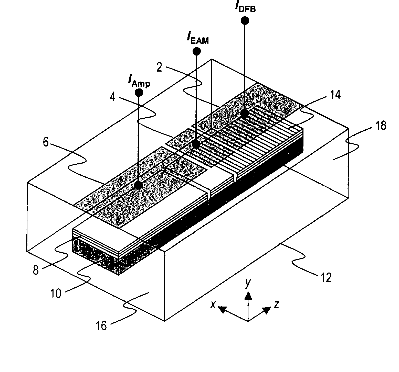
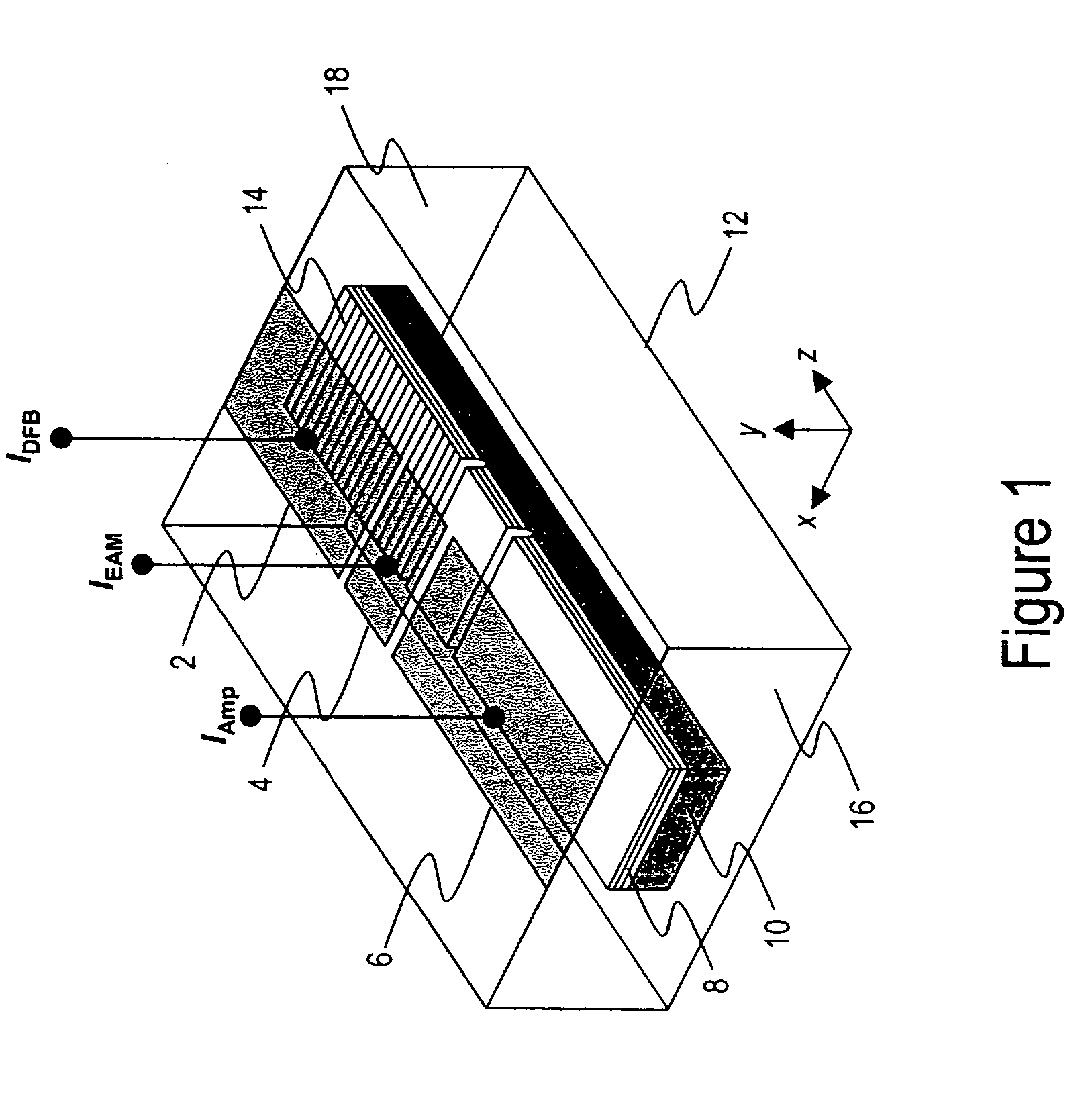
[0057] Currently, the laser source that is best suited for long-wavelength telecommunication applications is an electro-absorption modulated, amplified DFB laser 1, as shown in FIG. 1. The structure consists typically of a DFB section 2 coupled to a modulator 4 section and an amplifier 6 section. The DFB 2, and the mod...


PUM


Abstract

The present invention is a planar waveguide surface emitting laser (PWSEL) and photonic integrated circuit (PIC) technology. The PWVCL can stand alone or it can be integrated with a variety of optical devices, such as tuners, electro-optic or electro-absorption modulators (EOM or EAM), optical amplifiers (OA), waveguide or traveling wave photo detectors (WPD or TWPD), narrow or broadband filters, active or passive waveguides, and waveguide splitters or couplers to form photonic integrated circuits. Most or all of the components share the same transverse waveguide. A lateral index step or other suitable technique completes the waveguide so that light is guided in the longitudinal direction. Optical taps (reduced reflectivity mirrors) allow for surface emission of the light.

Description

[0001] This application claims the benefit of U.S. Provisional Application No. 60 / 404,350, filed Aug. 19, 2002.[0002] 1. Field of the Invention[0003] The present invention relates to designs, systems and methods of a semiconductor laser and, more particularly, to a planar waveguide surface emitting laser (PWSEL) and photonic integrated circuit (PIC) technology.[0004] 2. Description of the Related Art[0005] It has been goal long since the creation of the semiconductor integrated circuit, and later after the creation of the semiconductor laser, to create a photonic, integrated circuit, whereby each device of the integrated circuit or chip uses photons in some way. To date enormous effort and investment has been expended in the pursuit of creating a photonic integrated circuit with mediocre results. Conventional opto-electronic systems utilize and are implemented with hybrid components selected specifically and individually to optimize interaction between devices and overall performanc...

Claims


Application Information

Patent Timeline
IPC IPC(8): H01S5/026H01S5/12H01S5/125H01S5/183
CPCH01S5/026H01S5/0265H01S5/10H01S5/1032H01S5/12H01S5/1209H01S5/18341H01S5/141H01S5/18302H01S5/18308H01S5/18311H01S5/18319H01S5/125H01S5/18
Inventor WASSERBAUER, JOHN G.
Owner WASSERBAUER JOHN G
Why Eureka
Try Eureka