In-plane switching liquid crystal display with high aperture ratio

Inactive Publication Date: 2004-06-10
HANNSTAR DISPLAY CORPORATION
View PDF2 Cites 20 Cited by
  • Summary
  • Abstract
  • Description
  • Claims
  • Application Information

AI Technical Summary

Problems solved by technology

Furthermore, there is a problem that the number of the process steps is too many because the electrodes are formed in each substrate and the two substrates have a short point for applying voltages into the

Method used


Image

  • In-plane switching liquid crystal display with high aperture ratio
  • In-plane switching liquid crystal display with high aperture ratio
  • In-plane switching liquid crystal display with high aperture ratio

Examples


Example

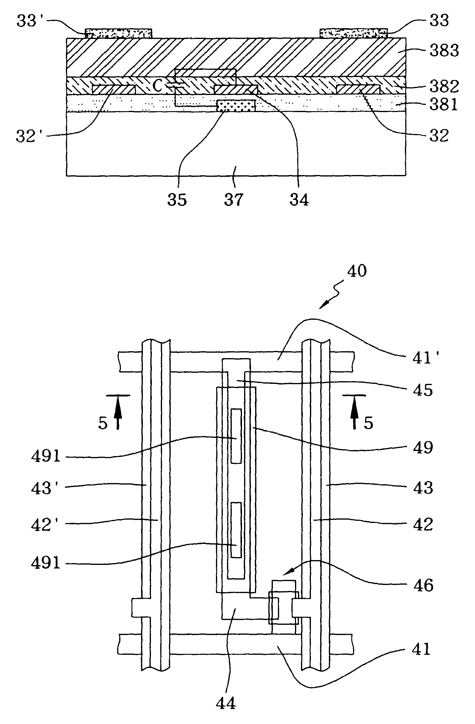
[0029] Referring to FIG. 3(a), the pixel 30 of the IPS LCD, in accordance with the first embodiment of the present invention, is shown. A pair of gate bus lines 31 and 31' is formed on a transparent insulating substrate such as a glass substrate in a transverse direction, and the gate electrode 35 extended from the gate bus lines 31' of the adjacent pixel goes towards the gate bus lines 31. A pixel electrode 34 completely overlaps with the gate electrode 35 from the middle of the gate bus lines 31' to the position close to gate bus lines 31, and is wider than the gate electrode 35. The signal bus lines 32 and 32' separately cross the gate bus lines 31 and 31' on two longitudinal sides of the pixel 30 in transverse direction. A switching element 36 formed in the pixel 30 is a three-terminal thin film transistor whose one terminal is connected to the pixel electrode 34 and the other two terminals are separately connected to the gate bus line 31 and the signal bus line 32. One common e...

Example

[0036] FIG. 4(a) shows a schematic layout diagram of the IPS LCD in accordance with the second embodiment of the present invention. A pair of gate bus lines 41 and 41' is formed on a transparent insulating substrate such as a glass substrate in a transverse direction, and the gate electrode 45 extended from the gate bus lines 41' of the adjacent pixel goes towards the gate bus lines 41. A first pixel electrode 44 completely overlaps with the gate electrode 45 from the middle of the gate bus lines 41' to the position close to gate bus lines 41, and is wider than the gate electrode 45. The signal bus lines 42 and 42' separately cross the gate bus lines 41 and 41' on two longitudinal sides of the pixel 40 in transverse direction. A switching element 46 formed in the pixel 40 is a three-terminal thin film transistor whose one terminal is connected to the first pixel electrode 44 and the other two terminals are separately connected to the gate bus line 41 and the signal bus line 42. One ...


PUM


Abstract

The present invention discloses an in-plane switching (IPS) LCD having a plurality of pixels arranged in a matrix to be formed on a transparent insulating substrate. A region, bounded by a pair of gate bus lines and a pair of signal bus lines, defines a unit pixel region. Each common electrode overlaps with one of the signal bus lines in parallel. A gate electrode extended from an adjacent gate bus line goes toward the gate bus line of the pixel. A switching element formed in the pixel is a three-terminal thin film transistor whose one terminal is connected to a pixel electrode by passing through the middle of the pixel, and the other two terminals are respectively connected to the gate bus line and the signal bus line. The pixel electrode overlaps with the gate electrode in parallel, and the storage capacitor of the pixel is formed therebetween.

Description

[0001] 1. Field of the invention[0002] The present invention relates to a liquid crystal display (LCD), and more particularly, to an in-plane switching (IPS) LCD having a high aperture ratio.[0003] 2. Description of the Related Art[0004] Liquid crystal displays (LCD) are replacing other display devices, such as CRTs, and become the most outstanding flat panel displays. In view of the driving methods of the LCDs, which can be classified into a simple matrix type and an active matrix type.[0005] An active matrix type LCD has a plurality of switching elements having non-linear characteristics, and pixels of the LCDs are controlled by the switching elements. Examples of the switching elements are three-terminal thin film transistors (TFTs) and two-terminal thin film diodes such as metal-insulator-metal (MIM) devices.[0006] A commonly used TFT LCD comprises a substrate having pixel electrodes, an opposite substrate having a common electrode, and a liquid crystal material between these tw...

Claims


Application Information

Patent Timeline
IPC IPC(8): G02F1/1343G02F1/1362
CPCG02F1/134363G02F2201/40G02F1/136213
Inventor LEE, DEUK SU
Owner HANNSTAR DISPLAY CORPORATION
Why Eureka
Try Eureka