

Semiconductor device
a technology of semiconductor devices and semiconductors, applied in the direction of pulse techniques, electronic switching, transistors, etc., can solve the problems of inability to supply a sufficient voltage to the gate of the igbt, inability to obtain sufficient collector current, and the failure of the semiconductor device itsel
- Summary
- Abstract
- Description
- Claims
- Application Information
AI Technical Summary
Benefits of technology
Problems solved by technology
Method used
Image

Examples
first embodiment
[0018] First Embodiment
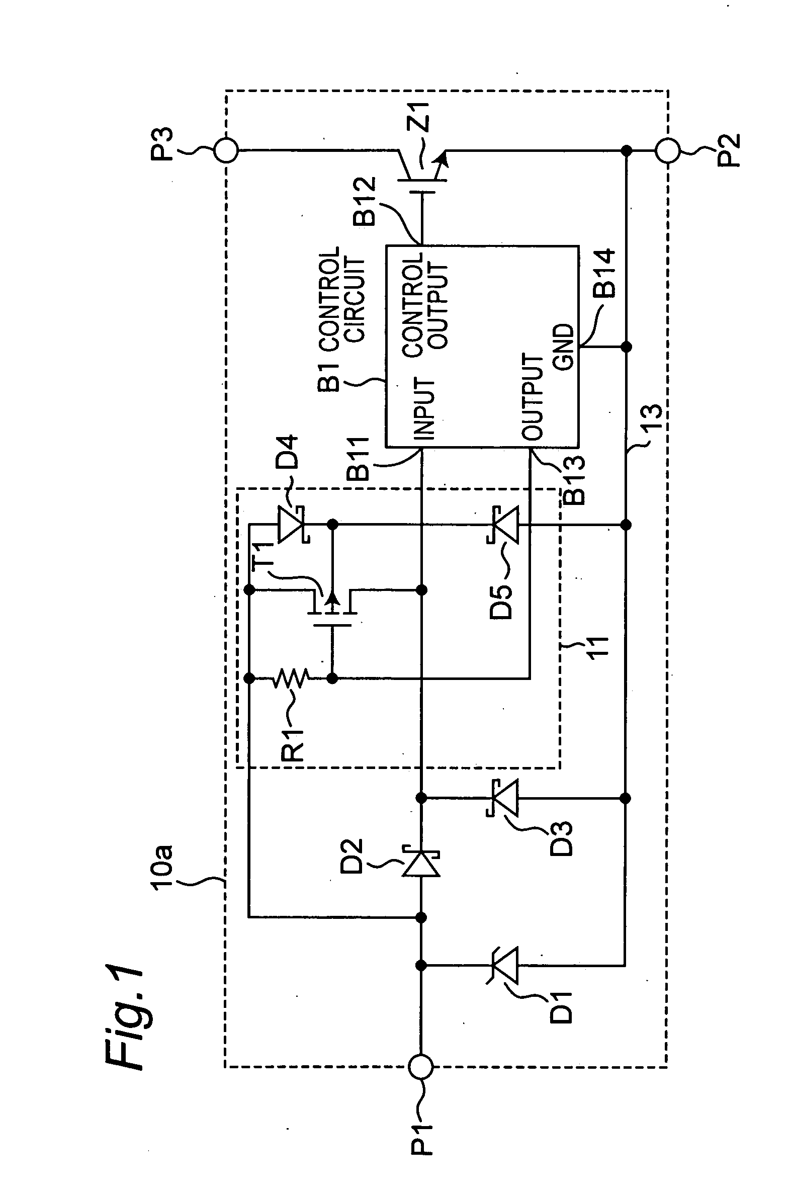
[0019] FIG. 1 shows a circuit configuration of a semiconductor device according to the first embodiment of the present invention.
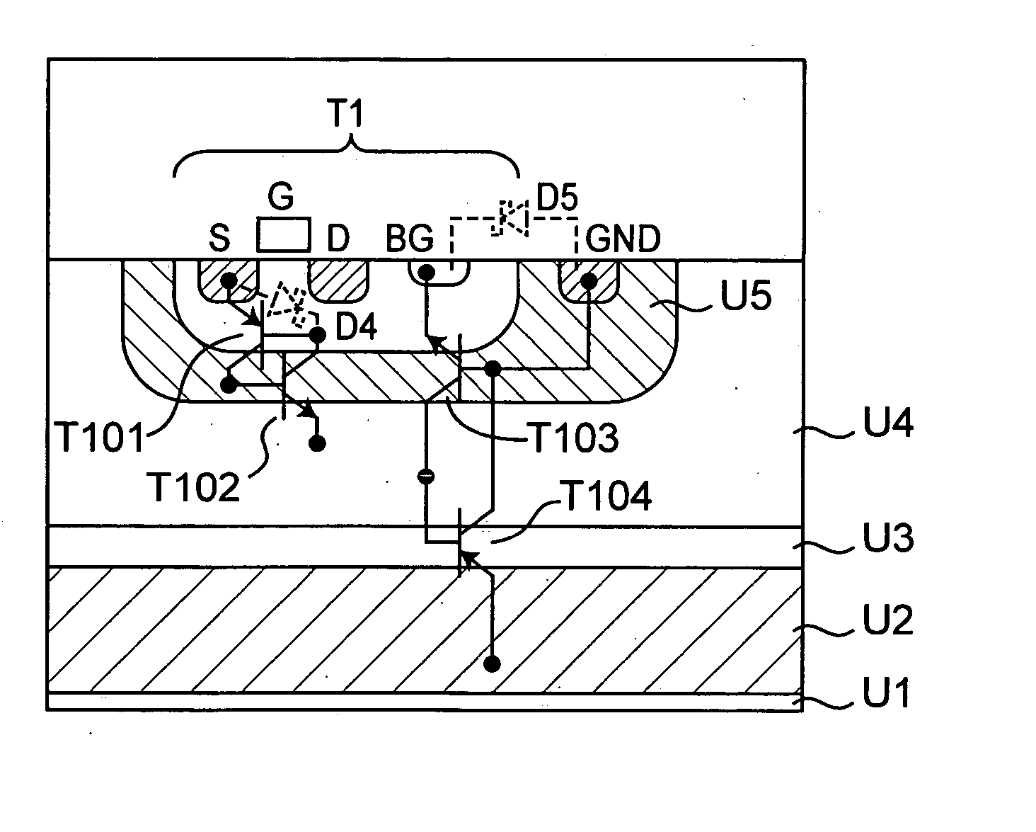
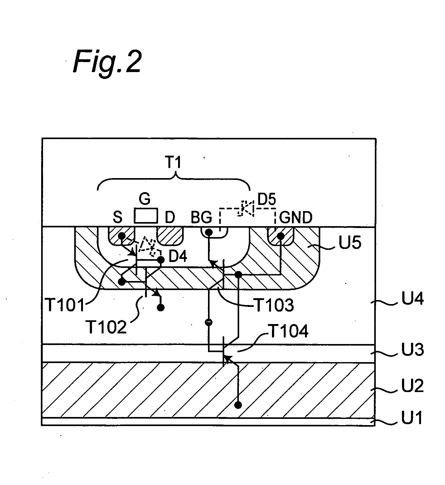
[0020] As shown in FIG. 1, a semiconductor device 10a according to this embodiment has an IGBT (Z1) and a control circuit B1 for driving the IGBT (Z1). The IGBT (Z1) and the control circuit B1 are formed on the same semiconductor substrate, and the control circuit B1 has a plurality of semiconductor elements. In order to prevent the parasitic thyristor generated with formation of the semiconductor element composing the control circuit B1 from being latched up, the semiconductor device 10a has a protecting circuit including a Zener diode D1 and Schottky barrier diodes D2 and D3. In addition, the semiconductor device 10a has a bypass circuit 11 including a resistor R1, a p-channel MOSFET (T1), and Schottky barrier diodes D4 and D5. The semiconductor device 10a has an input terminal P1, an emitter terminal P2, and a collector terminal P...
second embodiment
[0035] Second Embodiment
[0036] FIG. 3 shows the configuration of a semiconductor device according to the second embodiment of the present invention.
[0037] In a semiconductor device 10b according to this embodiment, a resistor R2 is serially inserted between the cathode of the Schottky barrier diode D2 and the input terminal B11 of the control circuit B1 in the configuration of the first embodiment. The resistor R2 operates to increase a voltage drop from the voltage of the input terminal P1 to the voltage of the input terminal B11 of the control circuit B1 when the p-channel MOSFET (T1) is in an OFF state.
[0038] A forward voltage drop caused by the Schottky barrier diode D2 is represented by V.sub.f(D2) [V], an ON resistance obtained when the p-channel MOSFET (T1) is in an ON state is represented by R.sub.on(t1) [.OMEGA.], the resistance of the resistor R2 is represented by R.sub.2 [.OMEGA.], and a current flowing into the input terminal B11 of the control circuit B1 at this time is...
third embodiment
[0040] Third Embodiment
[0041] FIG. 4 shows the configuration of a semiconductor device according to the third embodiment of the present invention.
[0042] A semiconductor device 10c according to this embodiment has a p-channel MOSFET (T2) in place of the resistor R2 in the configuration of the second embodiment. More specifically, the p-channel MOSFET (T2) is connected between the cathode of the Schottky barrier diode D2 and the input terminal B11 of the control circuit B1. The source and backgate of the p-channel MOSFET (T2) are connected to the cathode of the Schottky barrier diode D2, the drain of the Schottky barrier diode D2 is connected to the input terminal B11 of the control circuit B1, and the gate of the p-channel MOSFET (T2) is connected to the ground line 13.
[0043] Since the gate of the p-channel MOSFET (T2) is connected to the ground line 13, the p-channel MOSFET (T2) is turned on when a voltage which is equal to or more than the threshold voltage V.sub.th of the p-channe...
PUM
 Abstract
Description
Claims
Application Information