Electronic parts packaging structure and method of manufacturing the same

a technology of electronic parts and packaging structure, applied in the direction of printed circuit parts, association of printed circuit non-printed electric components, printed circuit components, etc., can solve the problems of circuit elements formed under the connection pads and in neighboring underlying areas thereof are damaged, and it is not possible that the connection pads under the via holes disappear

Active Publication Date: 2004-06-17
SHINKO ELECTRIC IND CO LTD
View PDF4 Cites 81 Cited by
  • Summary
  • Abstract
  • Description
  • Claims
  • Application Information

AI Technical Summary

Benefits of technology

[0015] In this manner, the via holes formed in the insulating film on the connection pads of the electronic parts are formed easily by the ordinary laser process to generate no trouble. As a result, the electronic parts packaging structure in which the electronic parts are face up mounted on the mounted body in a situation that they are buried in the insulating film, and the connection pads of the electronic parts are connected to the wiring patterns via the via holes is easily manufactured not to bring about an increase in cost at a high yield.

Problems solved by technology

Thus, upon forming the holes in the insulating film by the laser, such a trouble is caused that the exposed Al film is etched by the laser and scattered around peripheries, and in turn a part of the connection pads disappears.
For this reason, there is the problem that circuit elements formed under the connection pads and in neighboring underlying areas thereof are damaged by the laser.
Therefore, unlike the case where the connection pad the uppermost layer of which is made of the Al film is employed, it is not possible that the connection pads under the via holes disappear or the circuit elements under the connection pads and in neighboring underlying areas thereof are damaged.
As a result, the electronic parts packaging structure in which the electronic parts are face up mounted on the mounted body in a situation that they are buried in the insulating film, and the connection pads of the electronic parts are connected to the wiring patterns via the via holes is easily manufactured not to bring about an increase in cost at a high yield.

Method used


Image

  • Electronic parts packaging structure and method of manufacturing the same
  • Electronic parts packaging structure and method of manufacturing the same
  • Electronic parts packaging structure and method of manufacturing the same

Examples


first embodiment

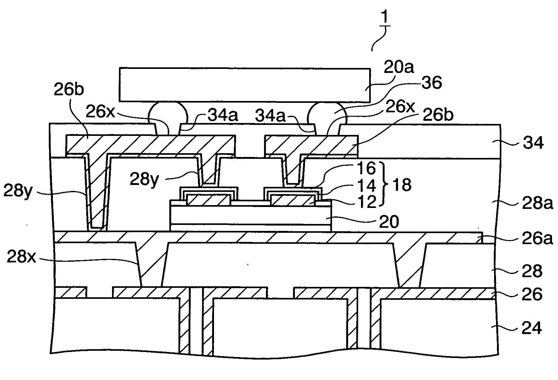
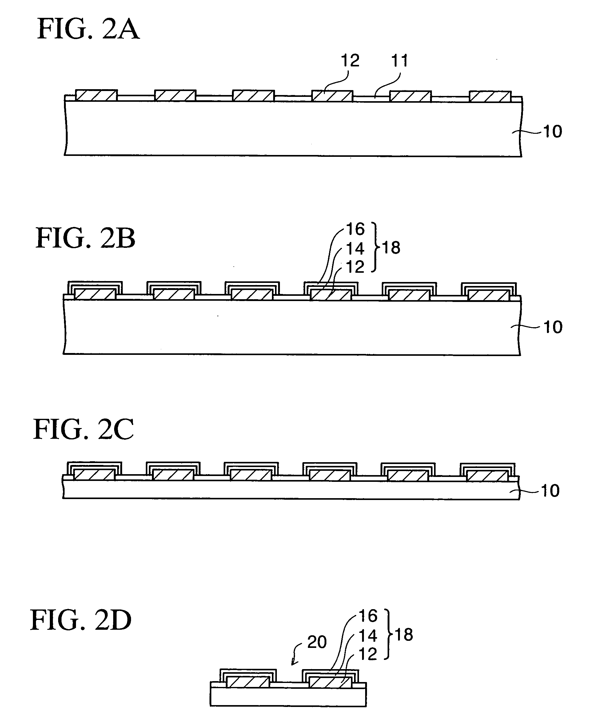
[0032] Next, a method of manufacturing an electronic parts packaging structure of a first embodiment of the present invention will be explained hereunder. FIGS. 2A to 2K are partial sectional views showing the method of manufacturing the electronic parts packaging structure of the first embodiment of the present invention. FIGS. 3 to 5 are partial sectional views showing variations of a connection pad according to the same electronic parts packaging structure.

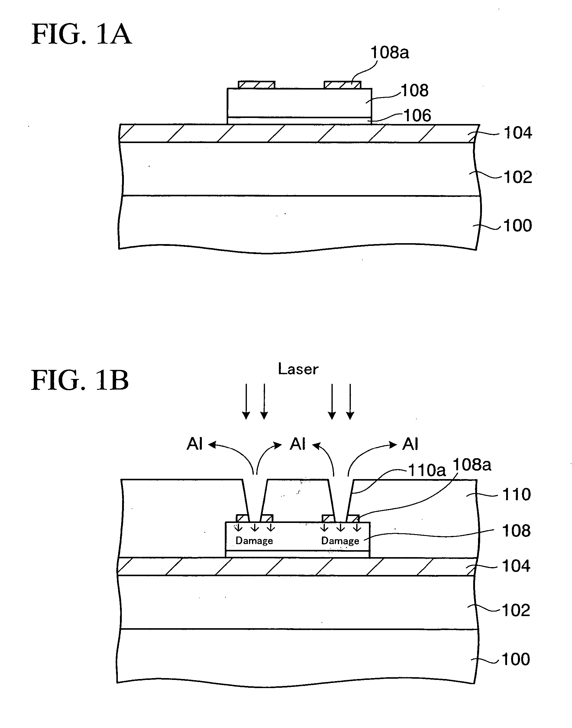
[0033] First, as shown in FIG. 2A, a silicon wafer (semiconductor wafer) 10 on which predetermined transistors, multi-layered wirings (not shown), etc. are formed and which has a thickness of about 400 .mu.m is prepared. Al pads 12 made of aluminum (Al) or Al alloy are exposed from an upper surface of the silicon wafer 10, and portions of the silicon wafer 10 except the Al pads 12 are covered with a passivation film 11 made of a silicon nitride film, polyimide resin, or the like.

[0034] Then, as shown in FIG. 2B, a nickel (Ni) f...

second embodiment

[0076] FIGS. 6A to 6G are partial sectional views showing a method of manufacturing an electronic parts packaging structure according to a second embodiment of the present invention. FIGS. 7A to 7C are partial sectional views similarly showing a variation 1 of a connection pad forming method according to the electronic parts packaging structure. FIGS. 8A to 8D are partial sectional views similarly showing a variation 2 of a connection pad forming method according to the electronic parts packaging structure.

[0077] A different point of the second embodiment from the first embodiment resides in that not the electroless plating but the photolithography is employed as the method of forming selectively the etching stopper layer on the Al pad 12. In FIGS. 6A to 6G, FIGS. 7A to 7C, and FIGS. 8A to 8D, detailed explanation of the same elements and the same steps as those in FIGS. 2A to 2K will be omitted herein.

[0078] In the method of manufacturing the electronic parts packaging structure ac...

third embodiment

[0097] FIGS. 9A to 9E are partial sectional views showing a method of manufacturing an electronic parts packaging structure of a third embodiment of the present invention. A different point of the third embodiment from the first embodiment is that the etching stopper layer in the laser process is formed by forming the conductive paste on the Al pads 12. In the third embodiment, detailed explanation of the same steps as those in the first embodiment will be omitted herein.

[0098] In the method of manufacturing the electronic parts packaging structure of the third embodiment of the present invention, first, as shown in FIG. 9A, the silicon wafer 10 (semiconductor wafer) having the same Al pads 12 as the first embodiment thereon is prepared. Then, as shown in FIG. 9B, a conductive paste film 38 is formed selectively on the Al pads 12. For example, the conductive paste film 38 is formed by coating the conductive paste material on the Al pads 12 by virtue of the screen printing, or the li...


PUM

PropertyMeasurementUnit
thicknessaaaaaaaaaa
thicknessaaaaaaaaaa
thicknessaaaaaaaaaa

Abstract

There is provided a electronic parts packaging structure that includes a mounted body on which an electronic parts is mounted, the electronic parts having a connection pad, which has an etching stopper film (a copper film, a gold film, a silver film, or a conductive past film) as an uppermost film, and mounted on the mounted body to direct the connection pad upward, an interlayer insulating film for covering the electronic parts, a via hole formed in the insulating film on the connection pad of the electronic parts, and a wiring pattern connected to the connection pad via the via hole.

Description

[0001] 1. Field of the Invention[0002] The present invention relates to an electronic parts packaging structure and a method of manufacturing the same and, more particularly, an electronic parts packaging structure in which electronic parts are packaged on a wiring substrate in a state that such electronic parts are buried in an insulating film and a method of manufacturing the same.[0003] 2. Description of the Related Art[0004] The development of the LSI technology as a key technology to implement multimedia devices is proceeding steadily to a higher speed and a larger capacity of the data transmission. According to this, a higher density of the packaging technology as interfaces between the LSI and electronic devices is also proceeding.[0005] In reply to the request of further higher density, there is the semiconductor device in which the semiconductor chips are mounted on the wiring substrate in a state that they are buried in the insulating film. As an example, in Patent Applica...

Claims


Application Information

Patent Timeline
Patent Type & Authority Applications(United States)
IPC IPC(8): H05K3/46H01L21/60H01L23/48H01L23/538H01L25/065H01L25/07H01L25/18H05K1/18
CPCH01L21/78Y10T29/49144H01L24/24H01L24/81H01L24/82H01L2224/16237H01L2224/24051H01L2224/24225H01L2224/24226H01L2224/32225H01L2224/73267H01L2224/8121H01L2224/81815H01L2224/92244H01L2924/01002H01L2924/01004H01L2924/01005H01L2924/01011H01L2924/01012H01L2924/01013H01L2924/01027H01L2924/01029H01L2924/01033H01L2924/01046H01L2924/01057H01L2924/01078H01L2924/01079H01L2924/19041H01L2924/19043H01L2924/30105H05K1/185H05K3/4602H05K2201/09509H01L2924/01006H01L2924/01024H01L2924/01047H01L2924/014H01L23/5389Y10T29/4913Y10T29/49165Y10T29/49126H01L2224/32245H01L2224/81192H01L2924/10253H01L2924/00H01L24/03H01L24/05H01L2224/02379H01L2224/05001H01L2224/05022H01L2224/05023H01L2224/05027H01L2224/05548H01L2224/82039H01L2924/12042H01L2224/05644H01L2924/00014H01L2224/05655H01L2224/05124H01L2224/05139H01L2224/05144H01L2224/05147H01L2224/05155H01L2224/05166H01L2224/05171H01L23/48
Inventor SUNOHARA, MASAHIROMURAYAMA, KEIMASHINO, NAOHIROHIGASHI, MITSUTOSHI
Owner SHINKO ELECTRIC IND CO LTD
Why Eureka
Try Eureka