Method and apparatus for forming a high quality low temperature silicon nitride film

Active Publication Date: 2004-06-24
APPLIED MATERIALS INC
View PDF33 Cites 127 Cited by
  • Summary
  • Abstract
  • Description
  • Claims
  • Application Information

AI Technical Summary

Problems solved by technology

Unfortunately, as transistor gate lengths are continually scaled, the transistors electrical characteristics and performance can greatly change due to thermal redistribution of dopants in the device.
Unfortunately, present techniques of forming high quality silicon nitride films in a single wafer reactor uti

Method used


Image

  • Method and apparatus for forming a high quality low temperature silicon nitride film
  • Method and apparatus for forming a high quality low temperature silicon nitride film
  • Method and apparatus for forming a high quality low temperature silicon nitride film

Examples


Embodiment Construction

[0014] The present invention is a high quality silicon nitride film which can be formed at a low deposition temperature. In the following description numerous specific details, such as deposition and anneal equipment have been set forth in order to provide a thorough understanding of the present invention. However, one of ordinary skill in the art will realize that the invention may be practiced without these specific details. In other instances well known semiconductor processes have not been described in particular detail so as to avoid unnecessarily obscuring the present invention.

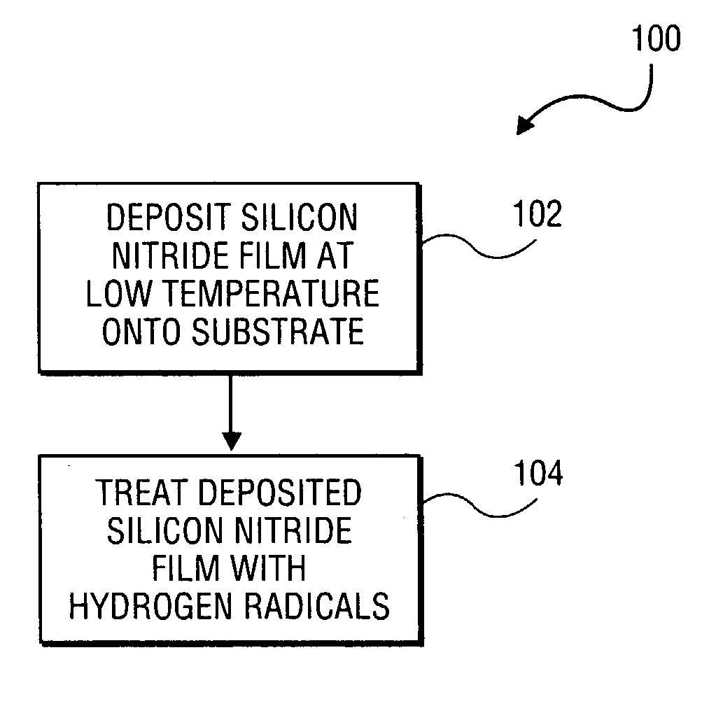
[0015] The present invention is a novel method and apparatus for forming a high quality silicon nitride film at a low deposition temperature of less than 550.degree. C. by thermal chemical vapor deposition (CVD). An example of a method of depositing a silicon nitride film is generally illustrated in the flow chart of FIG. 1. According to the first step of the present invention, as set forth in block 102...


PUM

PropertyMeasurementUnit
Temperatureaaaaaaaaaa
Timeaaaaaaaaaa
Pressureaaaaaaaaaa

Abstract

A method of forming a silicon nitride film is described. According to the present invention, a silicon nitride film is deposited by thermally decomposing a silicon/nitrogen containing source gas or a silicon containing source gas and a nitrogen containing source gas at low deposition temperatures (e.g., less than 550° C.) to form a silicon nitride film. The thermally deposited silicon nitride film is then treated with hydrogen radicals to form a treated silicon nitride film.

Description

[0001] 1. Field of the Invention[0002] The present invention relates to the field of thin film formation and more particularly to a method and apparatus for forming silicon nitride films at low deposition temperatures and high deposition rates.[0003] 2. Discussion of Related Art[0004] Modern integrated circuits are made up of literally millions and millions of transistors integrated together into functional circuits. In order to further increase the computational power or storage capability of integrated circuits, transistor feature size such as gate length and gate oxide thickness must be further scaled down. Unfortunately, as transistor gate lengths are continually scaled, the transistors electrical characteristics and performance can greatly change due to thermal redistribution of dopants in the device. As such, as devices are further scaled, the thermal budget used to manufacture the integrated circuit must also be reduced to insure consistent and reliable electrical performance...

Claims


Application Information

Patent Timeline
IPC IPC(8): C23C16/34C23C16/56H01L21/30H01L21/314H01L21/318H01L21/336
CPCC23C16/34C23C16/345C23C16/56H01L29/6659H01L21/3185H01L29/665H01L21/3003H01L21/02271H01L21/0217H01L21/022H01L21/0234
Inventor WANG, SHULINSANCHEZ, ERROL ANTONIO C.CHEN, AIHUA
Owner APPLIED MATERIALS INC
Why Eureka
Try Eureka