Base method treating method and electron device-use material

a technology of electron device and base method, which is applied in the direction of semiconductor devices, electrical devices, transistors, etc., can solve the problems of increasing power consumption, increasing leakage current, and increasing power consumption, so as to effectively terminate the dangling bond in si, improving the throughput of nitriding treatment, and improving the film quality of the thus formed nitride film

Inactive Publication Date: 2004-11-25
TOKYO ELECTRON LTD
View PDF23 Cites 34 Cited by
  • Summary
  • Abstract
  • Description
  • Claims
  • Application Information

AI Technical Summary

Benefits of technology

0142] The thus formed hydrogen radicals H* may easily penetrate or invade into the silicon nitride film 23, unlike hydrogen molecules, and they arrive at the interface between the Si substrate 21 and the silicon nitride film 23, to thereby effectively terminate the dangling bonds in Si.
0143] In this embodiment, it is

Problems solved by technology

This is because the leakage current of a certain degree can cause a severe problem in the recent devices which have attained finer structure, and/or higher performances, even when the leakage current of such a degree have actually caused substantially no problem in the conventional devices having a lower degree of integration.
However, when film thickness is reduced to 2 nm or less, an exponential increase in the leakage current is caused by the direct tunneling due to quantum effect, whereby the resultant power consumption is problematically increased.
Accordingly, in the field of a mobile terminal, it is an extremely important issue to accomplish the reduction in power consumption and to accomplish the above-mentioned high performances simultaneously.
Typically, for example, with respect to the development of the above-mentioned next-generation MOS transistor, when the microfabrication of a high-performance silicon LSI is investigated, there occurs a problem that the leakage current is increased and the resultant power consumption is also increased.
However, when the thickness of the convention

Method used


Image

  • Base method treating method and electron device-use material
  • Base method treating method and electron device-use material
  • Base method treating method and electron device-use material

Examples


Embodiment Construction

[0145] The nitride films which have been subjected to the above-mentioned respective evaluations corresponding to FIGS. 5-7, were manufactured by a method comprising the following steps.

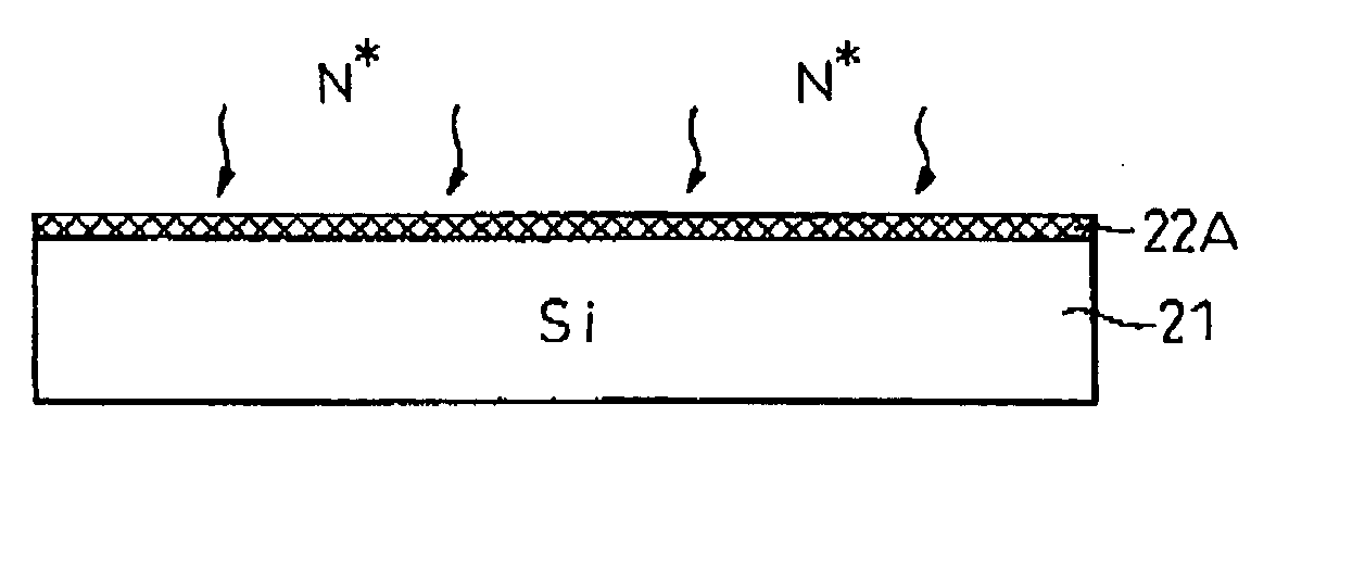
[0146] (1) Substrate

[0147] As the substrate, a 20 cm (8 inches) P-type silicon substrate was used, and the substrate had a specific resistance of 10 .OMEGA.cm, and a plane orientation of (100).

[0148] (2) Preliminary Washing Prior to Gate Oxidation

[0149] The natural oxide film and contaminating elements (metals, organic matters, particles) were removed by using the RCA-washing by use of a combination of APM (a liquid mixture of ammonia, aqueous hydrogen peroxide, and pure water=1:2:10; 60.degree. C.), HPM (a liquid mixture of hydrochloric acid, aqueous hydrogen peroxide, and pure water=1:1:10; 60.degree. C.) and DHF (a liquid mixture of hydrofluoric acid and pure water=1:100; 23.degree. C.). The RCA-washing was conducted in the sequence of APM (10 min.).fwdarw.pure water rinse (10 min.).fwdarw.DEF (3 ...


PUM


Abstract

A method of processing a for an electronic device, comprising, at least: a nitridation step (a) of supplying nitrogen radicals on the surface of the electronic device substrate, to thereby form a nitride film on the surface thereof; and a hydrogenation step (b) of supplying hydrogen radicals to the surface of the electronic device substrate. By use of this method, it is possible to recover the degradation in the electric property of an insulating film due to a turnaround phenomenon which can occur at the time of nitriding an Si substrate, etc.

Description

[0001] The present invention relates to a method of processing a substrate for electronic device by supplying nitrogen radicals, etc., to the electronic device substrate, and a material for an electronic device having a high-quality nitride film. The substrate-processing method according to the present invention may particularly suitably be used, e.g., for forming a high-dielectric film on an electronic device substrate.[0002] In general, the present invention is widely applicable to the production of materials for electronic device such as semiconductors or semiconductor devices, and liquid crystal devices. For the convenience of explanation, however, the background art relating to semiconductor devices as an example of the electronic devices, will be described here.[0003] Substrates for semiconductors or electronic device materials such as silicon have been subjected to various kinds of treatments such as formation of an insulating film such as oxide film, film formation by CVD (c...

Claims


Application Information

Patent Timeline
IPC IPC(8): H01L21/223H01L21/28H01L21/30H01L21/314H01L21/318H01L29/51
CPCH01L21/0217H01L21/02247H01L21/02332H01L21/0234H01L21/2236H01L21/28185H01L21/28202H01L21/3003H01L21/3144H01L21/3185H01L29/513H01L29/518
Inventor NAKANISHI, TOSHIOSUGAWARA, TAKUYAMOTONYAMA, SEIJISASAKI, MASARU
Owner TOKYO ELECTRON LTD
Why Eureka
Try Eureka