Optical module and a method of fabricating the same

a technology of optical modules and optical waveguides, applied in the direction of optical elements, semiconductor lasers, instruments, etc., can solve the problems of low manufacturing efficiency, inconvenient mass production of modules, and high connection accuracy between optical fibers and optical waveguides

Inactive Publication Date: 2004-07-01
TDK CORPARATION
View PDF15 Cites 19 Cited by
  • Summary
  • Abstract
  • Description
  • Claims
  • Application Information

AI Technical Summary

Problems solved by technology

However, when connecting terminal devices by optical fibers, it is necessary to provide a so-called optical module between the optical fiber and each terminal device, since terminal devices do not use optical signals but electric signals for information processing.
For this reason, there is a problem that manufacturing efficiency is low, so that the module is not suitable for mass production.
However, there is a problem that it is very expensive and requires high connection accuracy between the optical fiber and the optical waveguide.
However, this is not efficient for reducing hardware cost.
As explained above, the prior art optical module has certain problems such as low manufacturing efficiency because it requires fine tuning by a skilled worker and is very expensive.
Furthermore, there are problems that the system is enlarged and becomes high in cost when a large number of ONUs including the conventional optical module are installed in the CO.
It is possible to realize relatively low cost, which is not possible with the optical module including the conventional optical waveguide.
The optical module can be realized at relatively low cost, which is not possible with the optical module including a conventional optical waveguide.

Method used


Image

  • Optical module and a method of fabricating the same
  • Optical module and a method of fabricating the same
  • Optical module and a method of fabricating the same

Examples


Embodiment Construction

[0075] Preferred embodiments of the present invention will now be explained with reference to the drawings.

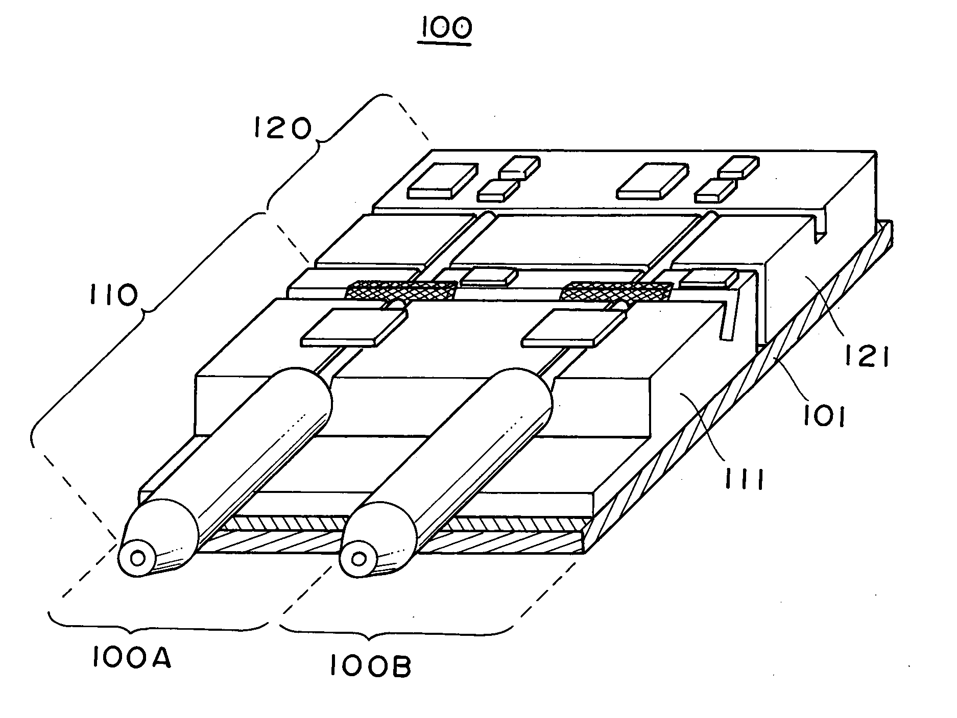
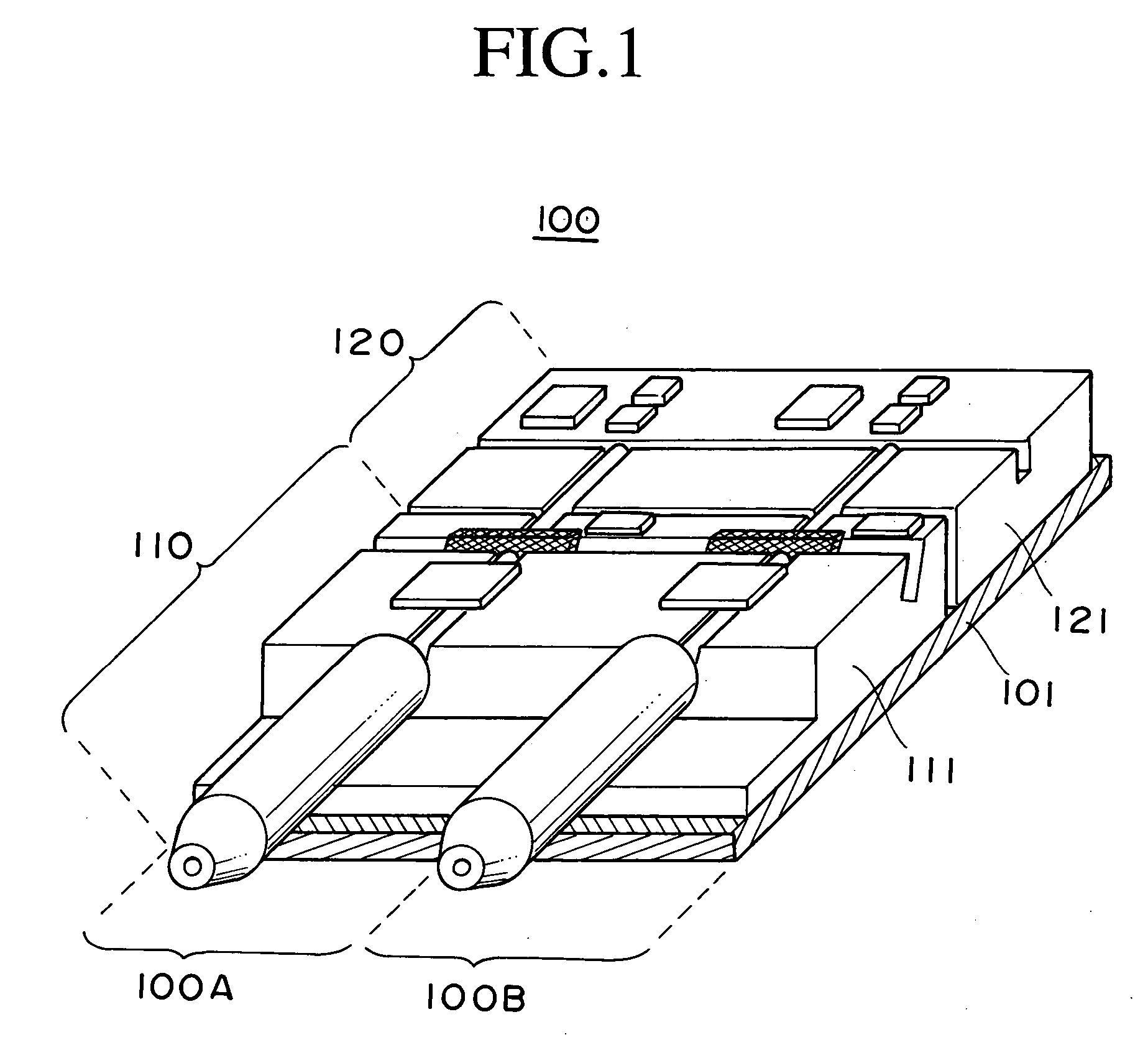
[0076] FIG. 1 is a simplified perspective view schematically showing the structure of an optical module 100 according to one preferred embodiment of the present invention.

[0077] As explained later in detail, the optical module 100 of this embodiment is finally encapsulated and the main portions covered with resin. FIG. 1 therefore shows the state with the resin removed from the optical module 100. Further, the transceiver ICs, leads and bonding wires are omitted in FIG. 1.

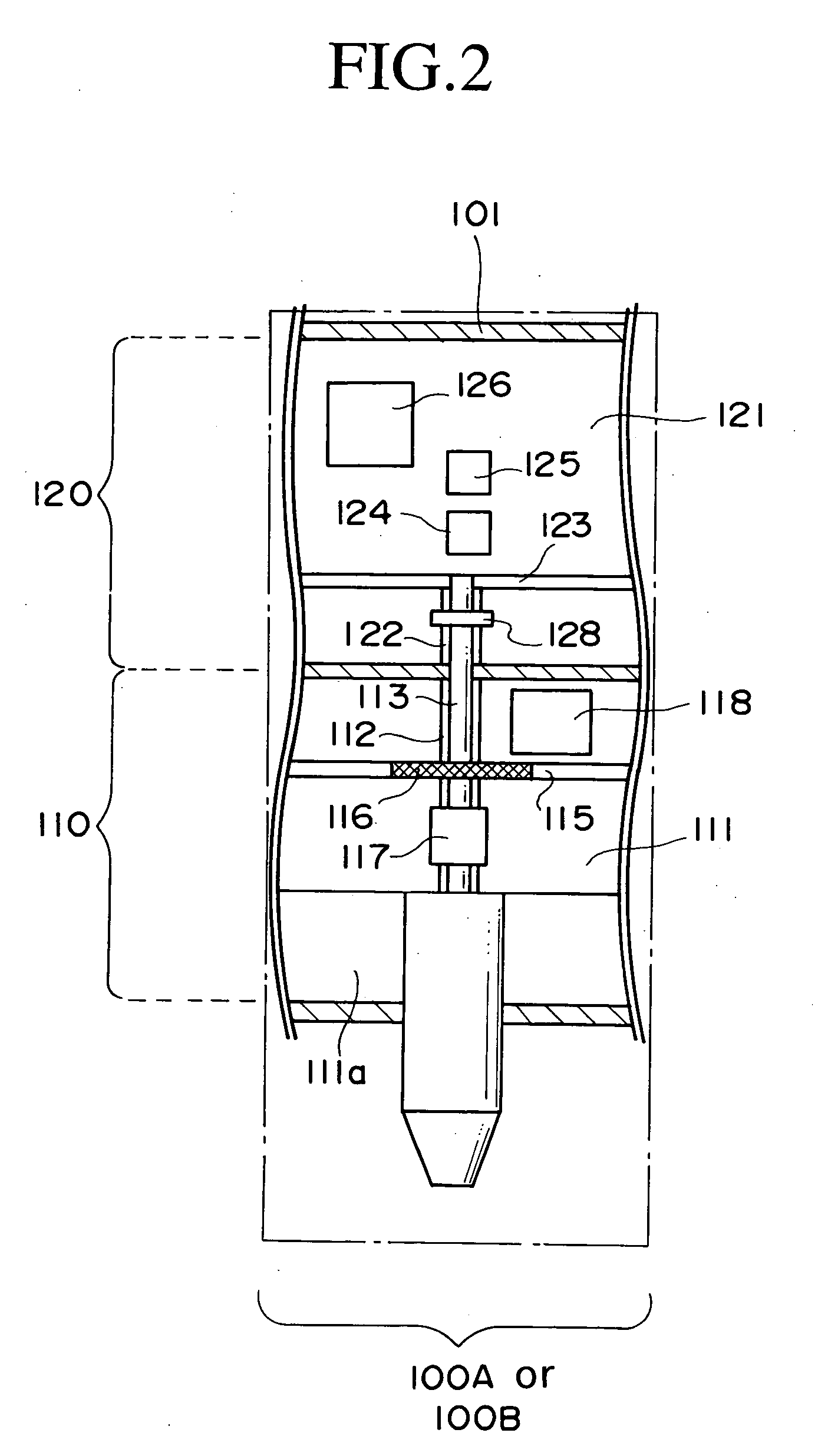
[0078] As shown in FIG. 1, the optical module 100 according to this embodiment has a PD (Photodiode) platform 110 and an LE (Light Emitter) platform 120 which are mounted on a die pad 101. The optical module 100 includes two transceiver units 100A and 100B, and each unit works as an independent element of the optical module.

[0079] The PD platform 110 and the LE platform 120 serve in common as platforms of the ...


PUM


Abstract

The present invention realizes miniaturization, low cost and improvement of fabricating efficiency of an optical module. The optical module 100 has a PD platform 110 and an LE platform 120 which are mounted on a die pad 101. The optical module 100 includes two transceiver units 100A and 100B, and each unit works as an independent element of the optical module. The PD platform 110 and the LE platform 120 are used in common by the two transceiver units 100A and 100B. The components of the two transceivers 100A and 100B are mounted on a single PD platform and a single LE platform.

Description

[0001] The present invention relates to an optical module and a method of fabricating the same, and more particularly, to an optical module which can be produced by an easy process and at low cost, and a method of fabricating the same.THE PRIOR ART[0002] The advent of the Internet allows one to access and manipulate huge quantities of information in real time. Copper wire, optical fiber, wireless means and the like are used to send and receive information. Optical fiber is especially superior for transmitting huge volumes of information at high speed. Thus, it is expected the optical fiber will be extended into every household in the future.[0003] However, when connecting terminal devices by optical fibers, it is necessary to provide a so-called optical module between the optical fiber and each terminal device, since terminal devices do not use optical signals but electric signals for information processing. The optical module transforms optical signals received from the optical fib...

Claims


Application Information

Patent Timeline
Patent Type & Authority Applications(United States)
IPC IPC(8): G02B6/38G02B6/42H01L31/0232H01S5/022H04B10/40H04B10/50H04B10/60H04B10/67H04B10/69
CPCG02B6/3826G02B6/3893G02B6/4292G02B6/4246G02B6/4206
Inventor LO, ADRIAN WING FAIHATA, KENJIROKINERI, TOHRUHANASHIMA, NAOKI
Owner TDK CORPARATION
Why Eureka
Try Eureka