

Nonvolatile semiconductor memory device
a memory device and non-volatile technology, applied in semiconductor devices, digital storage, instruments, etc., can solve the problems of inability to raise the integration degree of a memory device, inability to evaluate a correct current value, and inability to adapt to resistance changes
- Summary
- Abstract
- Description
- Claims
- Application Information
AI Technical Summary
Benefits of technology
Problems solved by technology
Method used
Image

Examples
Embodiment Construction
)
[0041] Embodiments of a nonvolatile semiconductor memory device of the present invention (hereafter properly referred to as "present invention device") are described below by referring to the accompanying drawings. A portion overlapped with that of a nonvolatile semiconductor memory device of the prior art is provided with the same symbol to describe it.
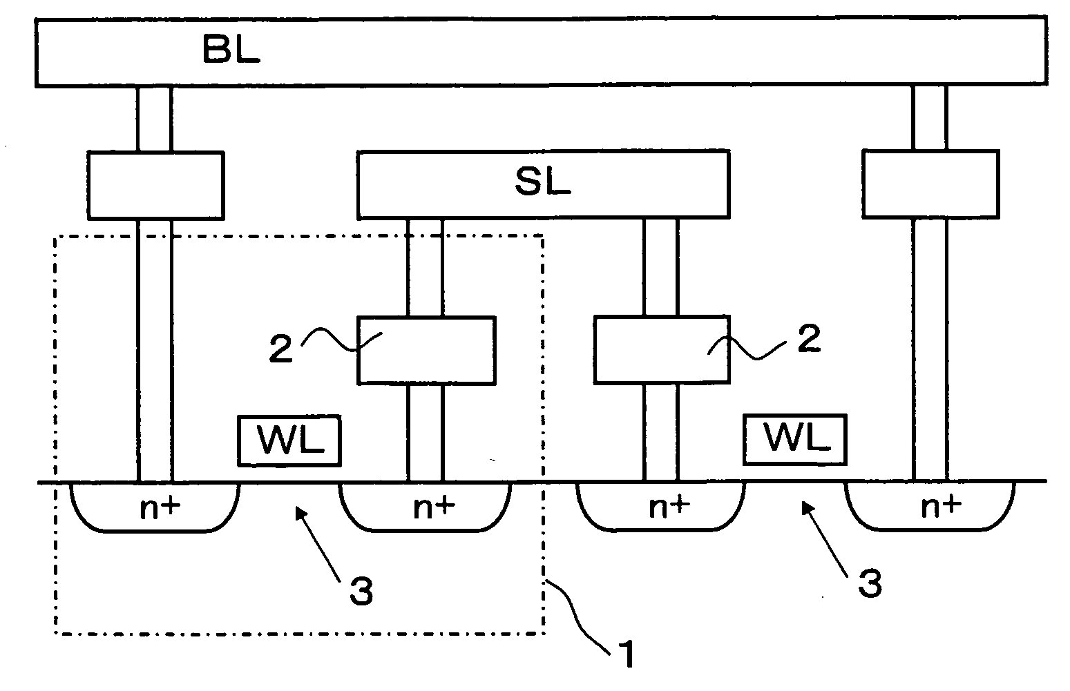
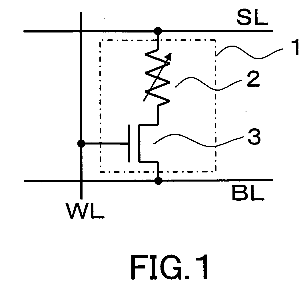
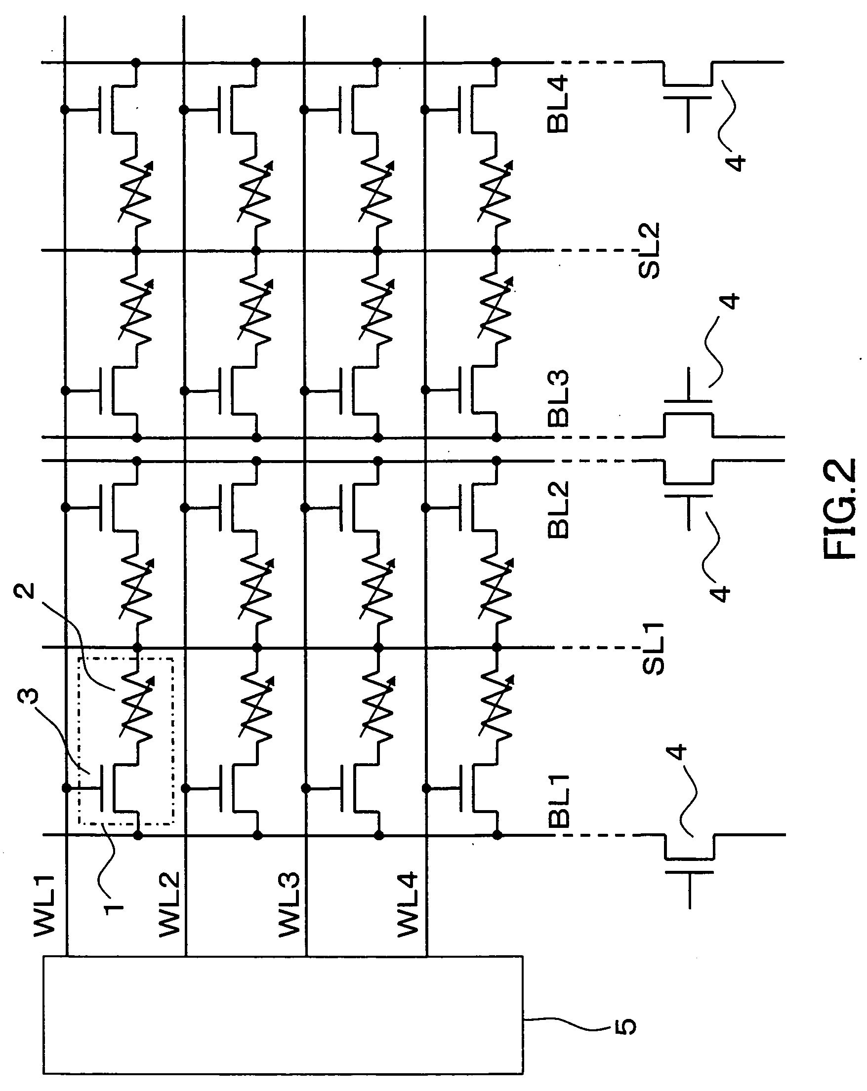
[0042] FIG. 1 shows a memory cell configuration of the present invention device. As shown in FIG. 1, a memory cell 1 is constituted by connecting one end of the RRAM device 2 serving as a variable resistive element with the source of the selection transistor 3 constituted by an N-type MOS transistor, and by connecting the drain of the selection transistor 3 with a bit line BL, the other end of the RRAM device 2 with a source line SL, and the gate of the selection transistor 3 with a word line WL. The memory cell has a configuration similar to the conventional memory cell configurations shown in FIG. 5 and FIG. 6 in that the variable...
PUM
 Abstract
Description
Claims
Application Information