Supercharge Your Innovation With Domain-Expert AI Agents!

Variable gain amplifier

a variable gain amplifier and amplifier technology, applied in the direction of gain control, amplifier modification to reduce non-linear distortion, amplification control details, etc., can solve the problems of difficult to design a cmos vga circuit having the operating frequency range of over 100 mhz, limited input/output signal level, and difficult to expect a smooth operation of vga for a low power supply

Inactive Publication Date: 2004-07-15
ELECTRONICS & TELECOMM RES INST
View PDF3 Cites 8 Cited by
  • Summary
  • Abstract
  • Description
  • Claims
  • Application Information

AI Technical Summary

Benefits of technology

The present invention provides a CMOS variable gain amplifier that can control the gain of input signals with low distortion and high linearity in a low voltage and high-speed operating range. It has a wideband characteristic and low power consumption. The invention solves the problem of limited device technology characteristics and the limitations of previous designs. It includes a first means for adjusting the transconductances of MOS transistors, a second means for adjusting the transconductances of MOS transistors, a third means for generating an output current with a stable bias current, and a fourth means for generating an output voltage with a variable gain. The invention provides a solution for designing a CMOS variable gain amplifier with low distortion, high linearity, low voltage operation, and high-speed operation.

Problems solved by technology

In particular, it is not easy to design a CMOS VGA circuit having the operating frequency range of over 100 MHz in view of device technology characteristics.
Furthermore, due to limitations in reduction of the threshold voltage in the MOS device, the input / output signal level is limited.
It is, thus, difficult to expect a smooth operation of VGA for a low power supply because of smaller input signal range.
Therefore, it is difficult to implement the CMOS variable gain amplifier with a low power consumption characteristics at the low voltage as an integrated circuit.

Method used


Image

  • Variable gain amplifier
  • Variable gain amplifier
  • Variable gain amplifier

Examples


Embodiment Construction

[0015] Reference will now be made in detail to the preferred embodiments of the present invention, examples of which are illustrated in the accompanying drawings, in which like reference numerals are used to identify the same or similar parts.

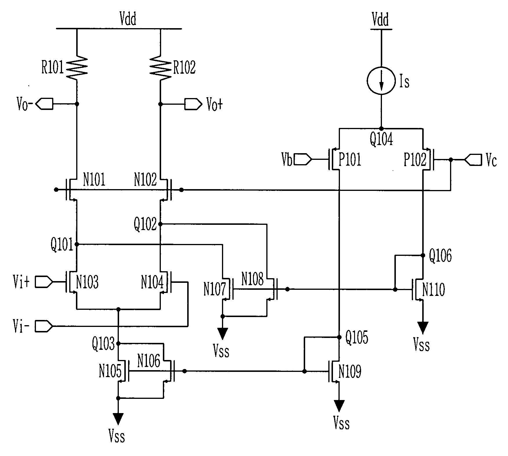
[0016] FIG. 1 is a circuit diagram illustrating the construction of a CMOS variable gain amplifier with low distortion, high linearity, low voltage operation and high-speed operation by the supply of a stabilized current bias according to a preferred embodiment of the present invention. The construction of the CMOS variable gain amplifier will be described below in detail with reference to FIG. 1.

[0017] A first resistor R101 and a first NMOS transistor N101 are connected in series between the power supply terminal Vdd and a first node Q101. A second resistor R102 and a second NMOS transistor N102 are connected in series between the power supply terminal Vdd and a second node Q102. The first and second NMOS transistors N101 and N102 are controll...


PUM


Abstract

Disclosed is a CMOS variable gain amplifier. The variable gain amplifier comprises a first means for first and second differential input voltages, a second means for controlling its transconductance to generate an output current according to a control voltage, a third means for a bias voltage to generate bias current by current mirror, and to supply a stabilized bias current to the second means using the replica current, and a fourth means for generating an output voltage with a variable gain according to control voltage by its output current generated in the second means. Therefore, the present invention provides a function of controlling low distortion and high linearity in low voltage and a high-speed operation by the supply of a stabilized sharing current bias, and can control a voltage gain in a wide range by the control voltage.

Description

[0001] 1. Field of the Invention[0002] The present invention relates to a CMOS variable gain amplifier (VGA), which can provide a function of controlling a gain of input signals with both low distortion and high linearity in a low voltage and a high-speed operating range by a stabilized sharing current bias.[0003] 2. Background of the Related Art[0004] Performance parameters of VGA that must be considered in designing the CMOS variable gain amplifier may include maximum of signal-to-noise ratio (SNR) for a desired signal value, a frequency bandwidth, low distortion, the input signal level that guarantees desired linearity, noise characterisitcs, gain control range, and the like. Further, its dependence on the temperature variation or supply voltage can not be excluded. In particular, it is not easy to design a CMOS VGA circuit having the operating frequency range of over 100 MHz in view of device technology characteristics. Furthermore, due to limitations in reduction of the thresho...

Claims


Application Information

Patent Timeline
Patent Type & Authority Applications(United States)
IPC IPC(8): H03G3/30H03F1/32H03F3/45H03G1/00
CPCH03F1/3211H03F3/45188H03G1/0029H03F2203/45398H03F2203/45702H03F2203/45288H03G3/30
Inventor KWON, CHONG KICHO, GYU HYUNGPARK, MUN YANGKIM, JONG DAE
Owner ELECTRONICS & TELECOMM RES INST
Features
  • R&D
  • Intellectual Property
  • Life Sciences
  • Materials
  • Tech Scout
  • Unparalleled Data Quality
  • Higher Quality Content
  • 60% Fewer Hallucinations
Learn More