Radiation detecting device and method of manufacturing the same

a technology of detecting device and detecting device, which is applied in the direction of radioation controlled device, television system, instruments, etc., can solve the problems of weak stress, improper installation position, and warpage of the layer

Inactive Publication Date: 2004-09-16
CANON KK
View PDF6 Cites 67 Cited by
  • Summary
  • Abstract
  • Description
  • Claims
  • Application Information

AI Technical Summary

Problems solved by technology

The radiation detection scintillator of the conventional example suffers from the following problems during the process or in an acceleration test of a long-term durability test.
(1) The respective structural layers are displaced due to a heat in a heat history during the process or during the durability, with the result that there arises such a problem that the respective layers are warped due to the displacement, an internal stress is applied to the phosphors and the respective structural layers, and a layer weak in the stress is destroyed or peeled off due to the internal stress.
There may arise such problems as an improper installation position or a connection failure due to the warp of the sensor panel in the case where a crimp type terminal is installed on an electrode lead pad potion on the panel for electric wiring connection.
Also, in some cases, the connection portion is damaged, and the connection fails due to the warp stress of the sensor panel during the acceleration durability.
(3) The sensor panel is flowed while the panel is mounted on a carrying holder, and in the case where the support substrate back surface comes in contact with a surface of the carrying holder, the light absorption is grazed and damaged or peeled off due to a mechanical friction in the case of the conventional material, with the result that the light shielding on the defective portion becomes insufficient, to thereby increase the image defects.

Method used


Image

  • Radiation detecting device and method of manufacturing the same
  • Radiation detecting device and method of manufacturing the same
  • Radiation detecting device and method of manufacturing the same

Examples


second example

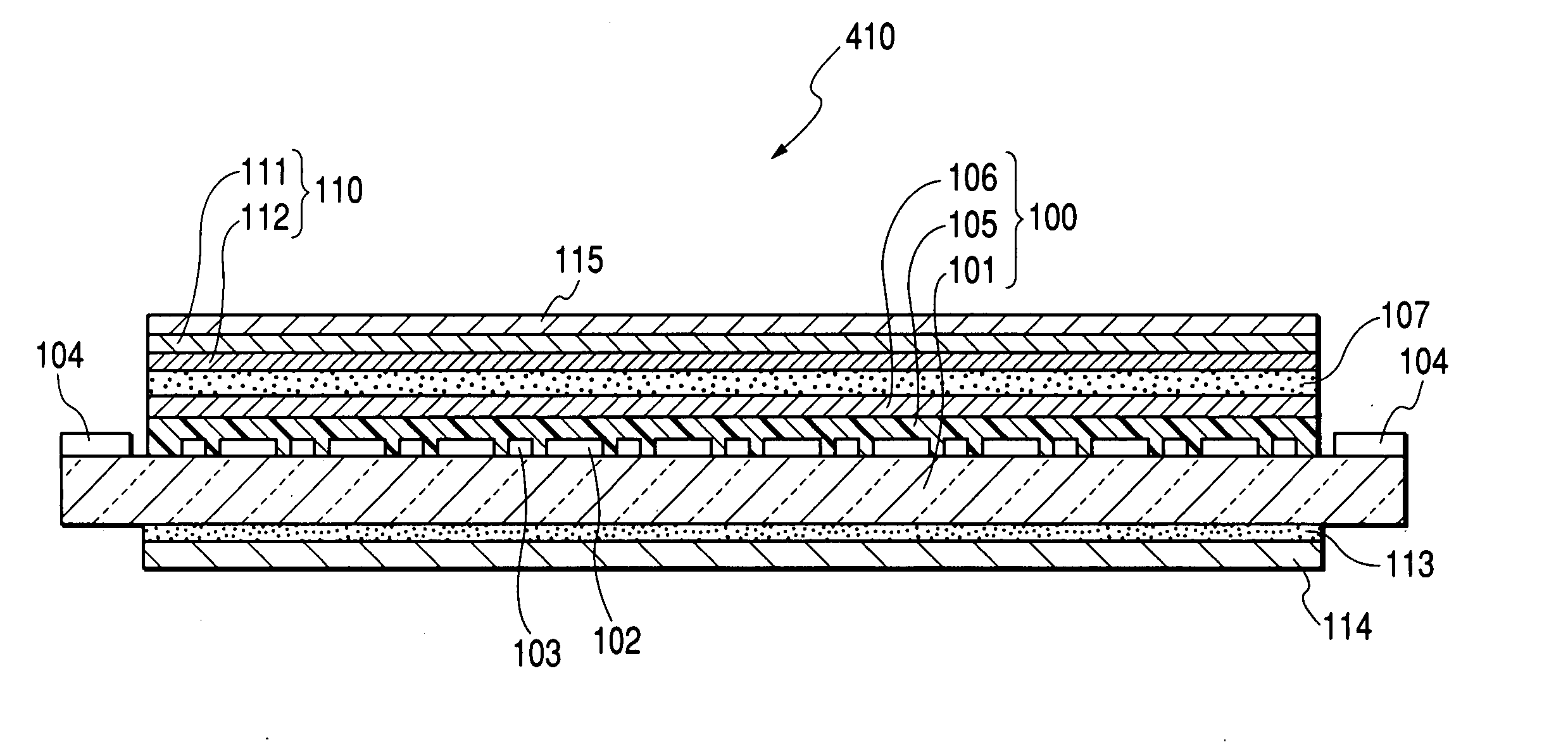
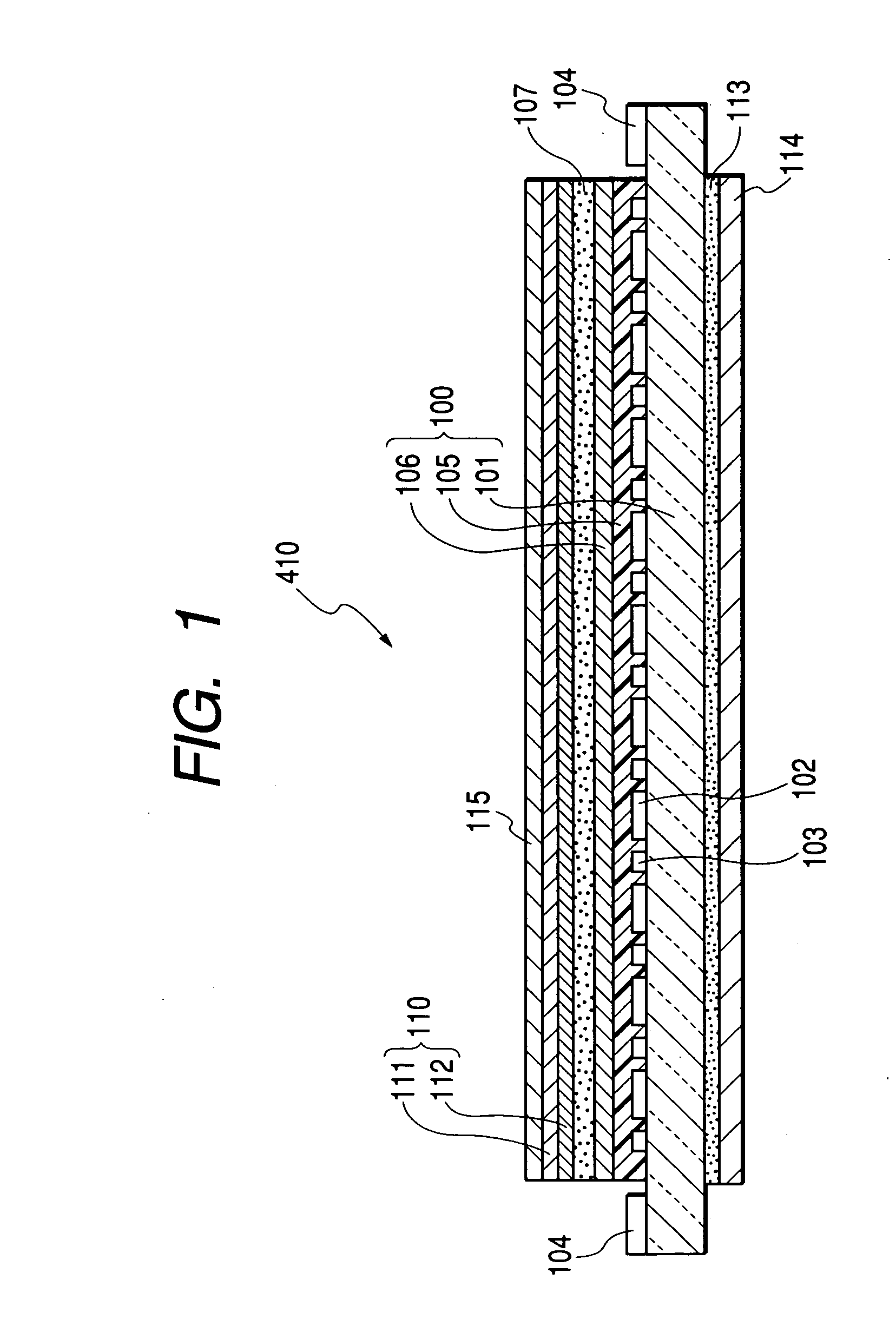
[0069] A photoelectric conversion element portion (pixel) 102 consisting of the photoelectric conversion elements and the TFTs are formed on a semiconductor thin film which is made of amorphous silicon on a glass substrate 101 as shown in FIG. 1, and a protective film 105 which is made of SiNx and a second protective layer 106 obtained by hardening a polyimide resin are formed on the photoelectric conversion element portion 102 to prepare a sensor panel 100.

[0070] A scintillator panel 110 and a moisture-proof protective layer 115 are prepared as in the first example.

[0071] An acrylic both-surface adhesive tape (made by Sumitomo 3M Corp., 9313) having a thickness of 50 .mu.m is bonded onto a black PET sheet having a thickness of 100 im (made by Panak) to prepare a PET sheet with an adhesive layer for bonding, to thereby obtain a warp correction layer 114 of 440 mm.times.440 mm having a light shielding function and a light absorption function.

[0072] The respective layers are bonded on...

third example

[0073] A photoelectric conversion element portion (pixel) 102 consisting of the photoelectric conversion elements and the TFTs are formed on a semiconductor thin film which is made of amorphous silicon on a glass substrate 101 as shown in FIG. 3, and a protective film 105 which is made of SiNx and a second protective layer 106 obtained by hardening a polyimide resin are formed on the photoelectric conversion element portion 102 to prepare a sensor panel 100.

[0074] Then, a phosphor layer 117 which is made of alkali halide and has been crystallized in the form of a column is formed in the thickness of 500 im on the sensor panel 100 through a vapor deposition method. Then, a protective layer that is made of polyparaxylylene resin is formed in the thickness of 10 .mu.m on the phosphor surface through the CVD method, an Al layer is then disposed in the thickness of 5000 .ANG. on the protective layer as a reflective layer through the sputtering method, and a protective layer which is made...


PUM


Abstract

In a radiation detecting device having a sensor panel in which a plurality of photoelectric conversion elements are formed on one surface of a support substrate, a moisture-proof protective layer is laminated on a surface of the sensor panel on which the photoelectric conversion elements are formed, and a warp correction layer is laminated on the other surface of the sensor panel, and the moisture-proof protective layer and the warp correction layer are formed of a resin film having a drawing or extrusion direction, respectively, and bonded together so as to make the drawing or extrusion directions of both the resin films similar to each other. With the formation of the radiation detecting device, the warp of the radiation detection panel induced by a thermal displacement is prevented.

Description

[0001] 1. Field of the Invention[0002] The present invention relates to a radiation detecting device that detects as an electric signal a radiation, which is employed in a medical diagnosis device, a nondestructive test device or the like, and a method of manufacturing the radiation detecting device. In the present invention, electromagnetic waves such as x-rays, .alpha.-rays, .beta.-rays and .gamma.-rays are also included in the radiation.[0003] 2. Related Background Art[0004] Up to now, an x-ray film system having a phosphor screen having x-ray phosphors therein and a both-side coated sensitizing agent has been generally employed for electrography. However, in recent years, from the viewpoints of such advantages that an image characteristic of a digital radiation detecting device having an x-ray phosphor layer and a two-dimensional sensor panel is excellent, and data is shared by downloading the data into a networked computer system because the data is digital data, the digital ra...

Claims


Application Information

Patent Timeline
Patent Type & Authority Applications(United States)
IPC IPC(8): G01T1/20G01T1/24G03B42/02H01L27/14H01L27/146H01L31/09H04N5/32
CPCG01T1/2018G01T1/244H01L27/14663H01L27/14618H01L2924/0002H01L2924/00G01T1/20
Inventor NAGANO, KAZUMITAMURA, TOMOYUKIOKADA, SATOSHITAKENAKA, KATSURO
Owner CANON KK
Why Eureka
Try Eureka