Method and device for the production of a silicon single crystal, silicon single crystal, and silicon semiconductor wafers with determined defect distributions

a technology of silicon semiconductor wafers and single crystals, which is applied in the direction of crystal growth process, polycrystalline material growth, chemistry apparatus and processes, etc., can solve the problems of difficult to deliberately adjust the radial crystal properties of single crystals, the flow of heat in the melt is extremely difficult to predict, and the diameter of single crystals with 200 mm or more is significan

Inactive Publication Date: 2004-09-30
SILTRONIC AG
View PDF13 Cites 60 Cited by
  • Summary
  • Abstract
  • Description
  • Claims
  • Application Information

AI Technical Summary

Benefits of technology

[0021] Especially with a view to the production of perfect silicon, tests have shown that the method according to the invention is particularly tolerant with respect to fluctuations of the pull rate. For instance, it is possible to pull. silicon single crystals with a diameter of at least 200 mm, which have no agglomerated point defects, even if the pull rate fluctuates by .+-.0.02 mm / min, particularly preferably .+-.0.025 mm / min or more, the fluctuation range referring to a single crystal of at least 30 mm. This fact increases the yield significantly, without the need to provide additional error-prone regulatory means to control the pull rate.
[0024] According to another embodiment of the invention, a bottom heater, which is conventionally present in pulling systems for the production of single crystals with diameters of at least 200 mm, is used for deliberately heating the melt from the center of the crucible bottom, thermal insulation being used to ensure that the bottom heater heats the center of the crucible bottom more strongly than the edge of the crucible bottom. To this end, a concentric gap filled with thermally insulating material is provided in an outer region of the baseplate and / or the outer crucible, so that the quartz crucible is thermally insulated more strongly in the outer region. The baseplate carries the crucible and a graphite outer crucible surrounding the latter. When heating is carried out with the bottom heater, therefore, heat is supplied to the melt essentially only at the center of the quartz-crucible bottom because of the annular thermal insulation in the baseplate or the outer crucible. For example, graphite sheets or graphite felts are suitable as an insulator material for filling the gap in the baseplate and / or in the outer crucible. The necessary bottom heater power is preferably in the range of from 20 kW to 80 kW, which is higher than the conventional powers. Thermal insulation may also be integrated into the crucible shaft, so as to minimize the downward thermal dissipation via the crucible shaft.
[0027] The aforementioned embodiments of the invention may be combined with measures which are already known and which are suitable for homogenizing the axial temperature gradient G(r). Preferred combinations are ones in which heat is additionally supplied to the phase boundary, which is formed by the growing single crystal, the atmosphere surrounding it, and the melt. This may, for example, be done by using a heat shield described in U.S. Pat. No. 6,153,008. It is particularly preferable to use a heating element on the lower edge of the heat shield, which is described in that patent application. A cooler acting on the single crystal may furthermore be fitted over the heating element, as described for example in U.S. Pat. No. 5,567,399. This makes it possible to increase the pull rate and to further adjust the radial homogenization of G.RTM.). The accelerated cooling associated with this furthermore makes the remaining COPs significantly smaller. The size of these COPs can thereby be brought below a critical value, below which these defects no longer have any effect on the component function.

Problems solved by technology

The production of single crystals which have a diameter of 200 mm or more represents a significant challenge, particularly since it is very difficult to deliberately adjust the radial crystal properties within a very narrow tolerance range.
The flows which transport heat in the melt are extremely difficult to predict.
They generally have a diameter of about 100 nm, and therefore cause problems for component fabrication.
These defects as well can also impair the functionality of the electronic components fabricated on silicon wafers.
This is not easy to achieve, however, especially when single crystals with a comparatively large diameter are being pulled, because the value of G then depends significantly on the radial position r. In general, owing to the radiative heat losses, the temperature gradient G is very much greater at the edge of the single crystal than at the center.
), can lead to there being several defect regions on a semiconductor wafer cut from a single crystal.
With the known prior art, however, sufficient radial V / G homogenization for the production of perfect silicon, especially with large crystal diameters, cannot be achieved in this way.
When analyzing the pulling tests which were carried out, it was found that insufficient radial homogenization of the ratio V / G.RTM.) is correlated with an inadequate heat supply from the melt to the center of the growth front.
They impede off-axial supply of heat to the melt.

Method used


Image

  • Method and device for the production of a silicon single crystal, silicon single crystal, and silicon semiconductor wafers with determined defect distributions
  • Method and device for the production of a silicon single crystal, silicon single crystal, and silicon semiconductor wafers with determined defect distributions
  • Method and device for the production of a silicon single crystal, silicon single crystal, and silicon semiconductor wafers with determined defect distributions

Examples


example 2

[0066] A silicon single crystal was produced, from which semiconductor wafers with the following properties could be separated:

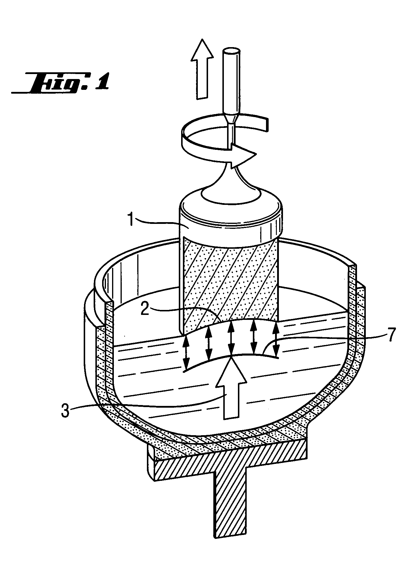
[0067] The semiconductor wafers were free of agglomerated self-point defects and two or more mutually separated axially symmetric regions, in which unagglomerated vacancies dominate as the defect type. The semiconductor wafers therefore have the properties of a silicon wafer corresponding to the section A in FIG. 15. The particular advantage of producing such semiconductor wafers is that the process management during the production of the single crystal is simplified, because less outlay is required on control technology. This is because there is a particularly wide process window in respect of the allowed variation of V / G. In the case of such semiconductor wafers, the oxygen precipitation occurring in the vacancy region can furthermore be adjusted accurately to the requirements of the component fabrication.

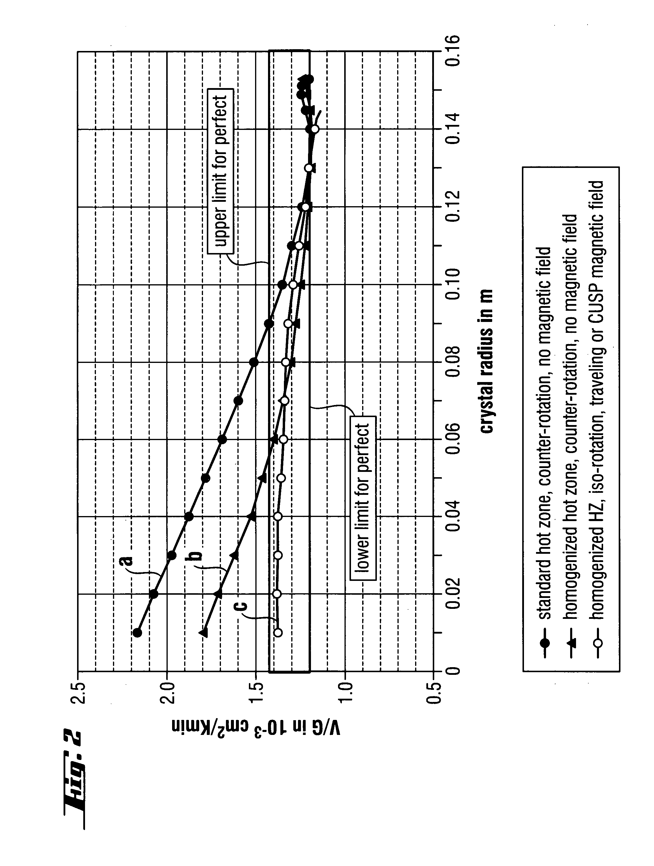
[0068] In this example, at the section position whi...

example 3

[0069] EXAMPLE 3

[0070] This example relates to semiconductor wafers with a defect distribution similar to that of the semiconductor wafers in Example 2, with the difference that unagglomerated interstitial silicon atoms dominate as the defect type in the two or more mutually separated axially symmetric regions. The process management during the production of the single crystal is simplified in the case of such semiconductor wafers as well, for the reasons mentioned above.

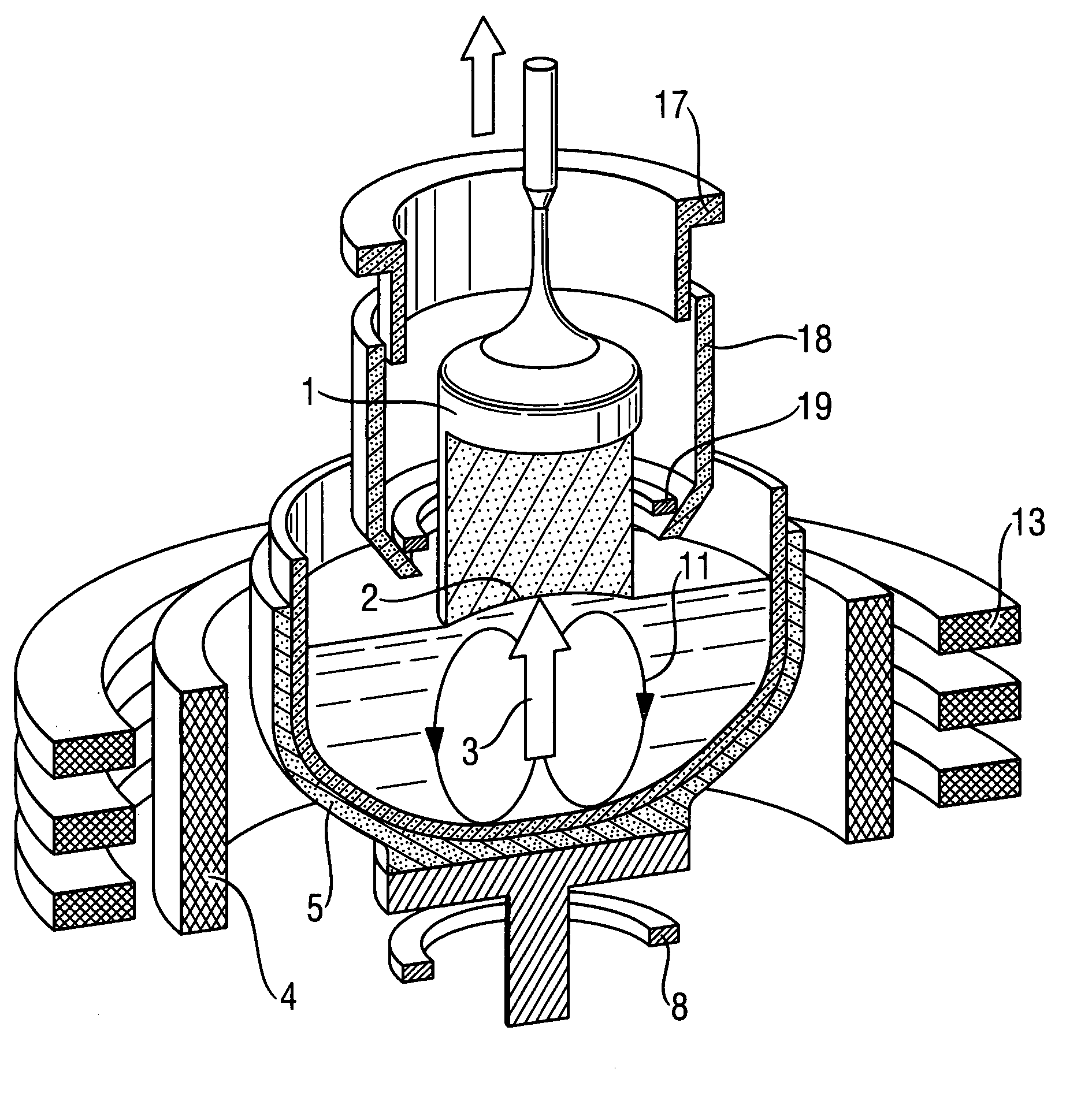
[0071] This distribution is illustrated in FIG. 17. The deliberate control of the heat distribution at the solidification front even makes it possible for a region 31 dominated by interstitial atoms to be produced at the center, or to be alternate with a vacancy-rich annular region 32 in a radial sequence.

[0072] The described distribution was achieved by a stronger heat supply at the center of the solidification front. To this end, the required heat flux was produced for each crystal position by means of the heating...


PUM

PropertyMeasurementUnit
diameteraaaaaaaaaa
electrical voltageaaaaaaaaaa
lengthaaaaaaaaaa

Abstract

A method for the production of a silicon single crystal by pulling the single crystal, according to the Czochralski method, from a melt which is held in a rotating crucible, the single crystal growing at a growth front, heat being deliberately supplied to the center of the growth front by a heat flux directed at the growth front. The method produces a silicon single crystal with an oxygen content of from 4*10<17 >cm<-3 >to 7.2*10<17 >cm<-3 >and a radial concentration change for boron or phosphorus of less than 5%, which has no agglomerated self-point defects. Semiconductor wafers are separated from the single crystal. These semiconductor wafers have may have agglomerated vacancy defects (COPs) as the only self-point defect type or may have certain other defect distributions.

Description

BACKGROUND OF THE INVENTION 1. Field of the Invention[0001] The invention relates to a method for the production of a silicon single crystal by pulling the single crystal, according to the Czochralski method, from a melt which is held in a rotating crucible, with the single crystal growing at a growth front. The invention also relates to a silicon single crystal and to semiconductor wafers which are separated therefrom. 2. The Prior Art[0002] The production of single crystals which have a diameter of 200 mm or more represents a significant challenge, particularly since it is very difficult to deliberately adjust the radial crystal properties within a very narrow tolerance range. This applies to the concentration of impurities or dopants, and especially to the crystal defects and self-point defects, and agglomerates thereof. Self-point defects include interstitial silicon atoms (silicon self-interstitials) and vacancies, which are formed at the growth front of the single crystal. The...

Claims


Application Information

Patent Timeline
Patent Type & Authority Applications(United States)
IPC IPC(8): C30B15/00C30B15/14C30B15/22C30B29/06
CPCC30B15/14C30B15/203Y10T117/1068C30B29/06C30B15/206C30B15/00
Inventor AMMON, WILFRIED VONVIRBULIS, JANISWEBER, MARTINWETZEL, THOMASSCHMIDT, HERBERT
Owner SILTRONIC AG
Why Eureka
Try Eureka