Substrate having a planarization layer and method of manufacture therefor, substrate for electro-optical device, electro-optical device, and electronic apparatus

a technology of planarization layer and substrate, applied in semiconductor/solid-state device testing/measurement, identification means, instruments, etc., can solve problems such as irregular surface of stacked structure of film formation layer, plurality of contact holes formed in interlayer insulating film, and defects in liquid crystal alignmen

Inactive Publication Date: 2004-10-21
SEIKO EPSON CORP
View PDF4 Cites 14 Cited by
  • Summary
  • Abstract
  • Description
  • Claims
  • Application Information

AI Technical Summary

Problems solved by technology

However, according to a film formation pattern of each layer, the surface of a stacked structure of film formation layers has irregularities.
When such irregularities occur in a layer being in contact with a liquid crystal layer, defects tend to occur in the alignment of liquid crystal.
Specifically, a problem occurs that

Method used


Image

  • Substrate having a planarization layer and method of manufacture therefor, substrate for electro-optical device, electro-optical device, and electronic apparatus
  • Substrate having a planarization layer and method of manufacture therefor, substrate for electro-optical device, electro-optical device, and electronic apparatus
  • Substrate having a planarization layer and method of manufacture therefor, substrate for electro-optical device, electro-optical device, and electronic apparatus

Examples


Embodiment Construction

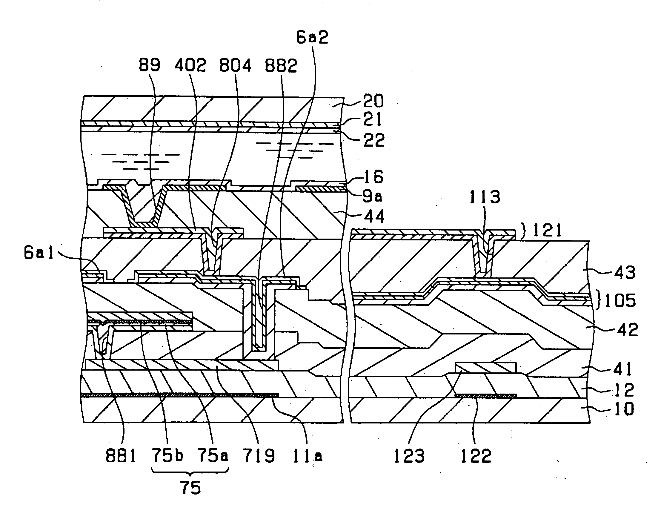
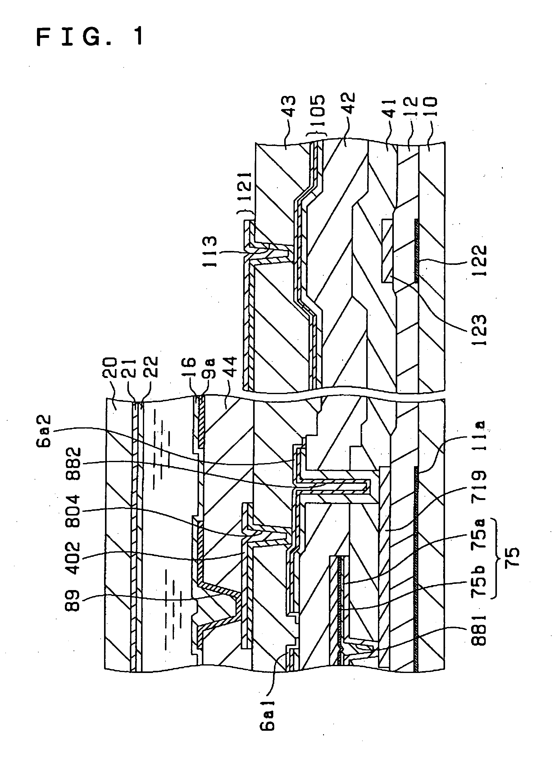
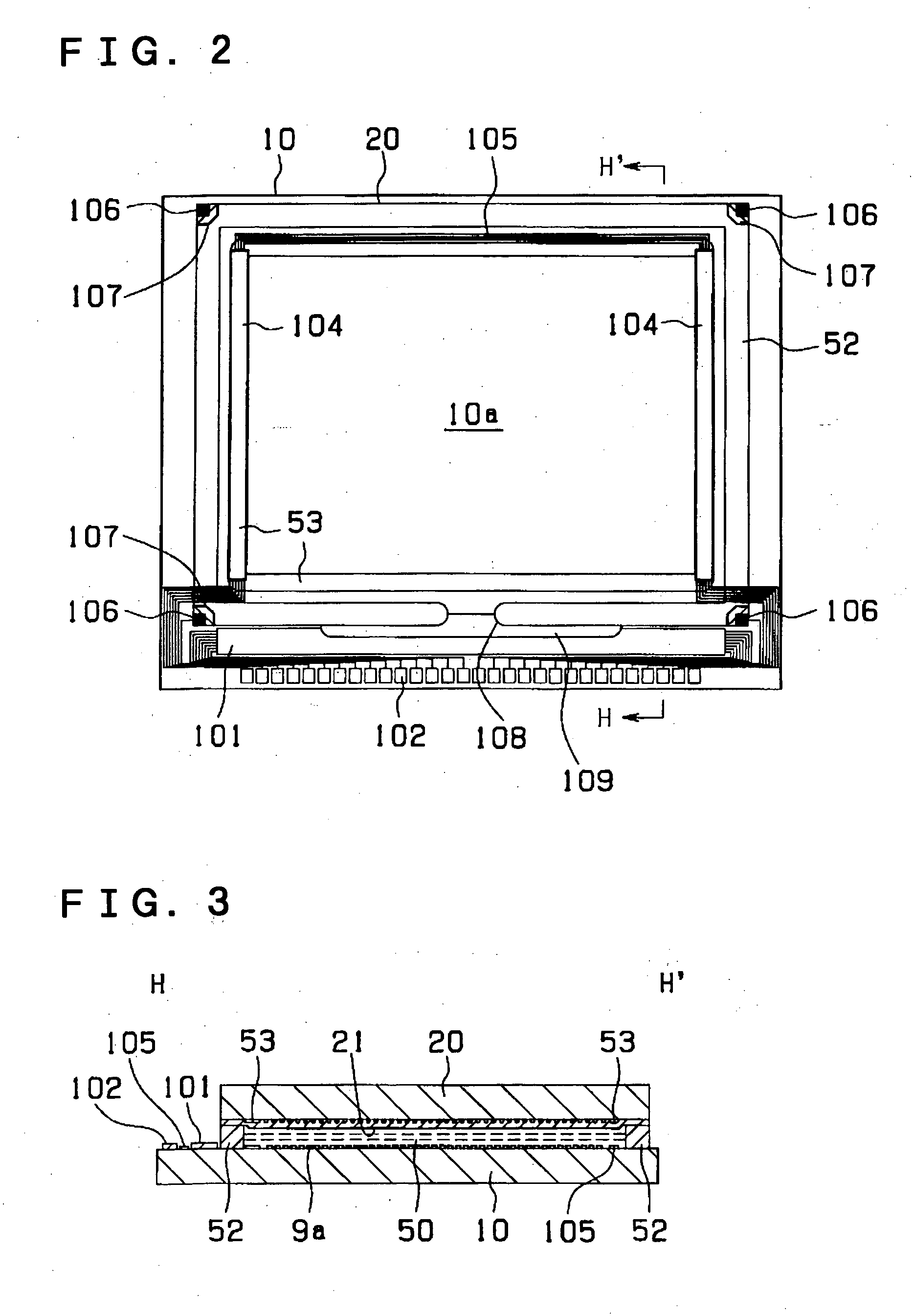
[0051] Reference will now be made in detail to the exemplary embodiments of the present invention in conjunction with the accompanying figures. FIG. 1 is a sectional view showing an element forming region and a wiring layer region of a substrate having a planarization layer according to one exemplary embodiment of the present invention. The present exemplary embodiment is configured to apply to a substrate for a liquid crystal device like a TFT substrate which is a substrate for an electro-optical device as a substrate having a planarization layer. FIG. 2 is a plan view from a counter substrate side showing a liquid crystal device which is an electro-optical device using a substrate for a liquid crystal device as a substrate for an electro-optical device according to the present exemplary embodiment, along with each component formed thereon. FIG. 3 is a sectional view from plane H-H' of FIG. 2 showing a liquid crystal device after a packaging step of adhering an element substrate an...


PUM


Abstract

A plurality of film formation layers where film formation patterns are formed, respectively, interlayer films which are formed between the plurality of film formation layers, respectively, a plurality of sub-interlayer-film wiring patterns, which are formed in film formation layers beneath the planarized interlayer films of the interlayer films, a plurality of contact holes formed in the planarized interlayer films in order to connect the plurality of sub-interlayer-film wiring patterns and the film formation patterns of layers above the planarized interlayer films, and one or more dummy patterns which are formed on a plurality of positions under the plurality of contact holes and which are formed in one or more film formation layers under the plurality of sub-interlayer-film wiring patterns, respectively so as to control the positions of the surfaces of the plurality of sub-interlayer-film wiring patterns.

Description

[0001] 1. Field of Invention[0002] The present invention relates to a substrate of a multilayer structure, especially a TFT substrate, and a substrate having a planarization layer suitable for a liquid crystal device, etc. using the TFT substrate and a manufacturing method thereof, and a substrate for an electro-optical device, and an electro-optical device.[0003] 2. Description of Related Art[0004] A liquid crystal device is constructed by filling liquid crystal between two sheets of substrates, such as a glass substrate or quartz substrate. A liquid crystal device can display images by providing active elements, such as a thin film transistor (hereinafter referred to as TFT) and pixel electrodes in a matrix shape on one substrate and counter electrodes (transparent electrodes (ITO (indium tin oxide))) on the other substrate, and changing optical properties of the liquid crystal layer filled between both substrates in response to image signals.[0005] An electro-optical device, such...

Claims


Application Information

Patent Timeline
IPC IPC(8): G02F1/136G02F1/1343G02F1/1362G02F1/1368G09F9/30H01L21/3205H01L21/336H01L23/52H01L29/786
CPCG02F1/136209G02F1/136227G02F1/136213G02F1/136
Inventor KURASHINA, HISAKI
Owner SEIKO EPSON CORP
Why Eureka
Try Eureka