Thin film transistor array panel, manufacturing method thereof, and mask therefor

a technology of thin film transistors and manufacturing methods, applied in the direction of identification means, semiconductor/solid-state device details, instruments, etc., can solve the problems of large contact resistance, frequent undercutting of blanket etching, and corrosion of al containing metals

Inactive Publication Date: 2004-11-11
SAMSUNG ELECTRONICS CO LTD
View PDF1 Cites 30 Cited by
  • Summary
  • Abstract
  • Description
  • Claims
  • Application Information

AI Technical Summary

Problems solved by technology

In the meantime, the contact between Al containing metal and ITO or IZO causes several problems such as corrosion of the Al containing metal and the large contact resistance.
However, the blanket etch frequently generates undercut formed by over-etching the Al containing metal under a sidewall of the contact hole.

Method used


Image

  • Thin film transistor array panel, manufacturing method thereof, and mask therefor
  • Thin film transistor array panel, manufacturing method thereof, and mask therefor
  • Thin film transistor array panel, manufacturing method thereof, and mask therefor

Examples


first embodiment

[0065] A TFT array panel for an LCD will be described in detail with reference to FIGS. 3 and 4 as well as FIGS. 1 and 2.

[0066] A TFT array panel for an LCD will be described in detail with reference to FIGS. 3 and 4 as well as FIGS. 1 and 2.

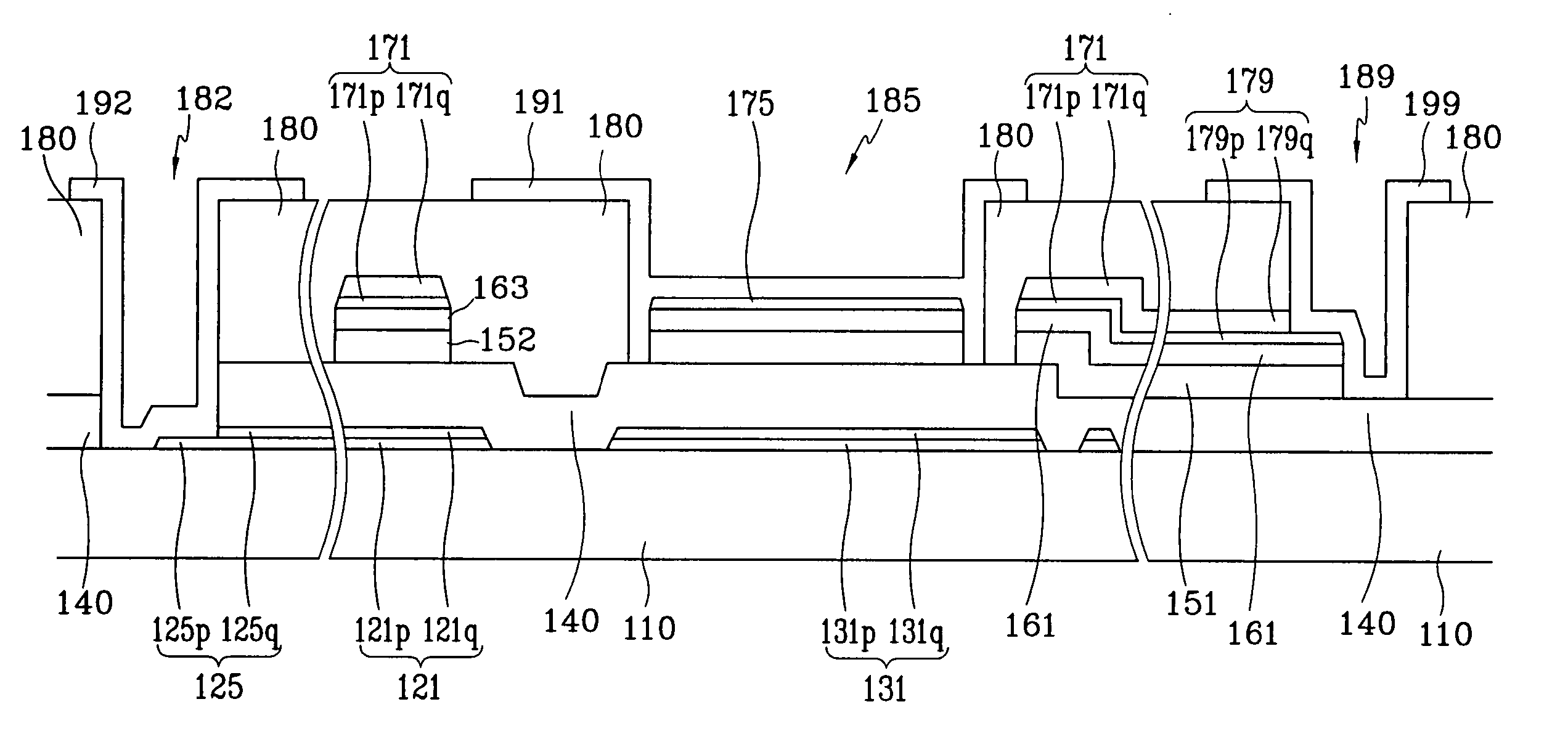
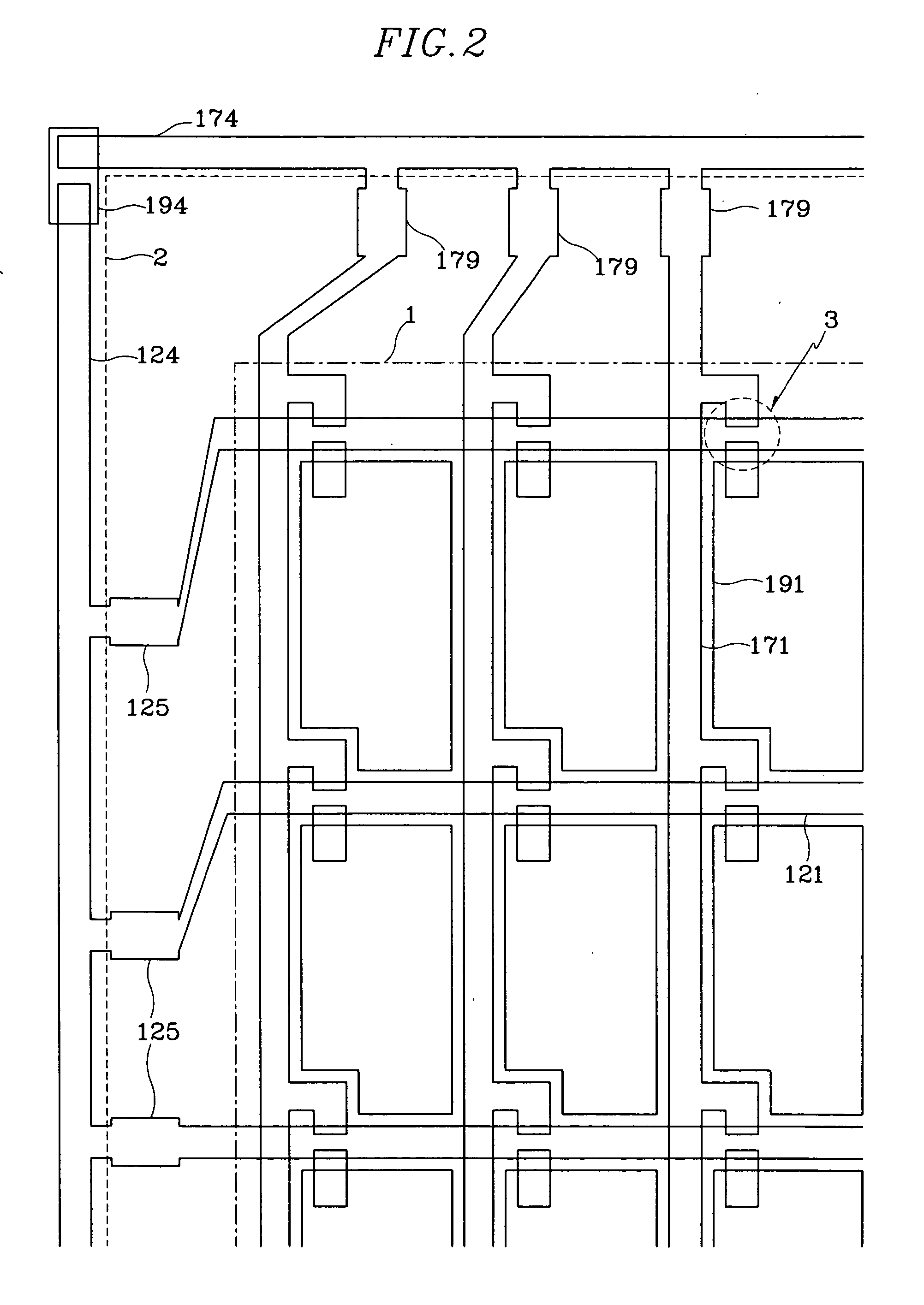
[0067] FIG. 3 is an exemplary layout view of TFTs, pixel electrodes, portions of signal lines located on the display area and expansions of the signal lines located on the peripheral area of the exemplary TFT array panel shown in FIG. 2 according to an embodiment of the present invention, and FIG. 4 is a sectional view of the TFT array panel shown in FIG. 3 taken along the line IV-IV'.

[0068] A plurality of gate lines 121 for transmitting gate signals and a gate shorting bar 124 extending substantially in a longitudinal direction are formed on an insulating substrate 110. Each gate line 121 extends substantially in a transverse direction and a plurality of portions of each gate line 121 form a plurality of gate electrodes 123. Each gate line 121 ...

1st embodiment

Method

[0094] A method of manufacturing the TFT array panel shown in FIGS. 1-4 according to an embodiment of the present invention will be now described in detail with reference to FIGS. 5A to 12 as well as FIGS. 1-4.

[0095] FIGS. 5A, 6A, 7A and 9A are layout views of the TFT array panel shown in FIGS. 1-4 in intermediate steps of a manufacturing method thereof according to an embodiment of the present invention, and FIGS. 5B, 6B, 7B and 9B are sectional views of the TFT array panel shown in FIGS. 5A, 6A, 7A and 9A taken along the lines VB-VB', VIB-VIB', VIIB-VIIB', and IXB-IXB', respectively. FIG. 8 is a sectional view of the TFT array panel shown in FIG. 7A taken along the line VIIB-VIIB' in the step of the manufacturing method following the step shown in FIG. 7B, and FIGS. 11 and 12 are sectional views of the TFT array panel shown in FIG. 9A in the steps of the manufacturing method following the step shown in FIG. 9B. FIG. 10 illustrates alignment between slits of a mask and a drai...

2nd embodiment

Method

[0121] Now, a method of manufacturing the TFT array panel shown in FIGS. 13-15 according to an embodiment of the present invention will be described in detail with reference to FIGS. 16A-25B as well as FIGS. 13-15.

[0122] FIG. 16A is a layout view of a TFT array panel shown in FIGS. 13-15 in the first step of a manufacturing method thereof according to an embodiment of the present invention; FIGS. 16B and 16C are sectional views of the TFT array panel shown in FIG. 16A taken along the lines XVIB-XVIB' and XVIC-XVIC', respectively; FIGS. 17A and 17B are sectional views of the TFT array panel shown in FIG. 16A taken along the lines XVIB-XVIB' and XVIC-XVIC', respectively, and illustrate the step following the step shown in FIGS. 16B and 16C; FIG. 18A is a layout view of the TFT array panel in the step following the step shown in FIGS. 17A and 17B; FIGS. 18B and 18C are sectional views of the TFT array panel shown in FIG. 18A taken along the lines XVIIIB-XVIIIB' and XVIIIC-XVIIIC'...


PUM

PropertyMeasurementUnit
distanceaaaaaaaaaa
inclination anglesaaaaaaaaaa
dielectric constantaaaaaaaaaa

Abstract

A passivation layer is deposited and a photoresist is formed. The photoresist includes first to third portions with decreased thickness, the second portions located on portions of drain electrodes and data lines and the third portions located on portions of gate lines. A mask for forming the photoresist has rectilinear slits with width and distance of about 0.8-2.0 microns on an area corresponding to the second portions. The passivation layer and an underlying semiconductor layer as well as the photoresist are etched to expose portions of the gate insulating layer under the third portions of the photoresist as well as portions of the passivation layer under the second portions of the photoresist. The exposed portions of the passivation layer and the gate insulating layer are removed to expose the drain electrodes, the gate lines and the data lines as well as portions of the semiconductor layer, which are subsequently removed.

Description

[0001] (a) Field of the Invention The present invention relates to a thin film transistor array panel, a manufacturing method thereof, and a mask therefor.[0002] (b) Description of the Related Art[0003] Liquid crystal displays (LCDs) are one of the most widely used flat panel displays. An LCD includes two panels provided with field-generating electrodes and a liquid crystal (LC) layer interposed therebetween. The LCD displays images by applying voltages to the field-generating electrodes to generate an electric field in the LC layer, which determines orientations of LC molecules in the LC layer to adjust polarization of incident light.[0004] Among LCDs including field-generating electrodes on respective panels, a kind of LCDs provides a plurality of pixel electrodes arranged in a matrix at one panel and a common electrode covering an entire surface of the other panel. The image display of the LCD is accomplished by applying individual voltages to the respective pixel electrodes. For...

Claims


Application Information

Patent Timeline
Patent Type & Authority Applications(United States)
IPC IPC(8): G02F1/1345G02F1/136G02F1/1343G02F1/1362G02F1/1368G03C5/00G03F1/00G03F1/14G03F9/00G09F9/30H01L21/00H01L21/28H01L21/3205H01L21/336H01L21/768H01L23/52H01L23/532H01L29/423H01L29/49H01L29/786
CPCG02F1/136227G03F1/14G02F2001/136236G03F1/00G02F1/136236
Inventor PARK, WOON-YONGLEE, WON-HEEKIM, IL-GONLIM, SEUNG-TAEKSONG, YOU-LEEJUN, SAHNG-IK
Owner SAMSUNG ELECTRONICS CO LTD
Why Eureka
Try Eureka