Vacuum processing method, vacuum processing apparatus, semiconductor device manufacturing method and semiconductor device

a vacuum processing and vacuum processing technology, applied in the field of vacuum processing methods, vacuum processing apparatuses, semiconductor device manufacturing methods and semiconductor devices, can solve the problems of uneven processing, inability to render vacuum processing characteristics further uniform in a broad range, and non-uniformity of film quality or change of film quality itself in the thickness direction

Inactive Publication Date: 2004-11-25
CANON KK
View PDF9 Cites 15 Cited by
  • Summary
  • Abstract
  • Description
  • Claims
  • Application Information

AI Technical Summary

Benefits of technology

[0081] While the effects of the present invention are sufficiently obtained by combining the two high-frequency powers as above, it is possible to further combine a third high-frequency power. As for the range of the third high-frequency power, there is no limitation as far as the first and second high-frequency powers are set within the appropriate ranges.
[0084] Furthermore, in the present invention, the above described electrode may be formed in a rod-like shape. In the case where the shape of the electrode is the rod-like shape capable of being handled substantially as one dimension, it is possible to acquire the effects of the present invention more remarkably since the power is not substantially diffracted laterally to the direction of travel so that no secondary standing wave occurs due to the lateral diffraction of the power.
[0085] Moreover, in the present invention, the above described article to be processed may be formed in a cylindrical or columnar shape. In the case where the article to be processed is formed in a cylindrical or columnar shape, reflection ends of the high-frequency power on the article to be processed are limited to both ends thereof. For that reason, the distribution of the standing waves becomes relatively simple compared with the case where many standing waves occur due to many reflection ends, so that it is possible to acquire the effects of the present invention further remarkably.
[0097] In addition, according to the present invention, it is possible to obtain a more remarkable effect by disposing the plurality of plasma generation high-frequency electrodes on the same circumference. The reason is presumably that, as a distance from the junction of the high-frequency powers to each high-frequency electrode can be rendered as equal as possible by disposing the plasma generation high-frequency electrodes on the same circumference, the effect of the present invention such as branching the powers not by leaning to a specific electrode and increasing the total power without generating an abnormal discharge can be rendered remarkable.
[0102] In addition, according to the present invention, as the electric field distribution in the entire areas in the reaction container including those on the electrodes is rendered uniform, it is no longer necessary to adopt an approach of having the material gases distributed to compensate for the nonuniformity of the electric field distribution in the reaction container as in the conventional techniques, so that it is possible to decrease the number of material gas introducing means to a minimum. Accordingly, it is preferable that the number of the means for introducing the gases into the reaction container should be one in consideration of the apparatus costs and operability. In the case of having just one gas introducing means, however, it is preferable to dispose the gas introducing means at the center of the reaction container since a more remarkable effect of the present invention can be obtained by rendering the positional relation among the gas distribution in the reaction container, the substrate supporting means, the reaction container and the plasma generation high-frequency electrode as symmetrical as possible.

Problems solved by technology

Consequently, it was difficult to render the vacuum processing characteristics further uniform in a broad range.
In addition, in the case of the device having a thick film thickness such as the electrophotographic photosensitive member, there were cases where the state of the plasma changes as the film was deposited so that distribution of characteristics in an in-plane direction of the substrate became different in the film thickness direction resulting in nonuniformity of the film quality or change of the film quality itself in the thickness direction.
Such nonuniformity is a serious problem in the case of forming a crystalline or non-single crystalline functional deposited film used not only for the electrophotographic photosensitive member but also for the photovoltaic devices, image input line sensors, imaging devices and so on.
In addition, the same processing unevenness will arise in plasma processing processes such as dry etching and sputtering in the case of rendering the discharge frequency higher, which will become a serious problem in practice if it remains as it is.
Although various improvements have been made in the electrode's shape, the form of applying the high-frequency power and so on in order to reduce such processing unevenness and render the uniformity higher, it has been by no means easy to maintain compatibility between the uniformity of the film thickness and that of the film quality and to acquire the deposited film having good film quality while maintaining the uniformity of the film thickness.
However, as a result of conducting an experiment on the uniformity of the vacuum processing characteristics by using the technology disclosed by Japanese Patent Application Laid-Open No. 60-160620, the inventors hereof could certainly improve the uniformity to a certain level but could not acquire the uniformity level that is required in recent years.

Method used


Image

  • Vacuum processing method, vacuum processing apparatus, semiconductor device manufacturing method and semiconductor device
  • Vacuum processing method, vacuum processing apparatus, semiconductor device manufacturing method and semiconductor device
  • Vacuum processing method, vacuum processing apparatus, semiconductor device manufacturing method and semiconductor device

Examples


exemplary experiment 1

[0298] (Exemplary Experiment 1)

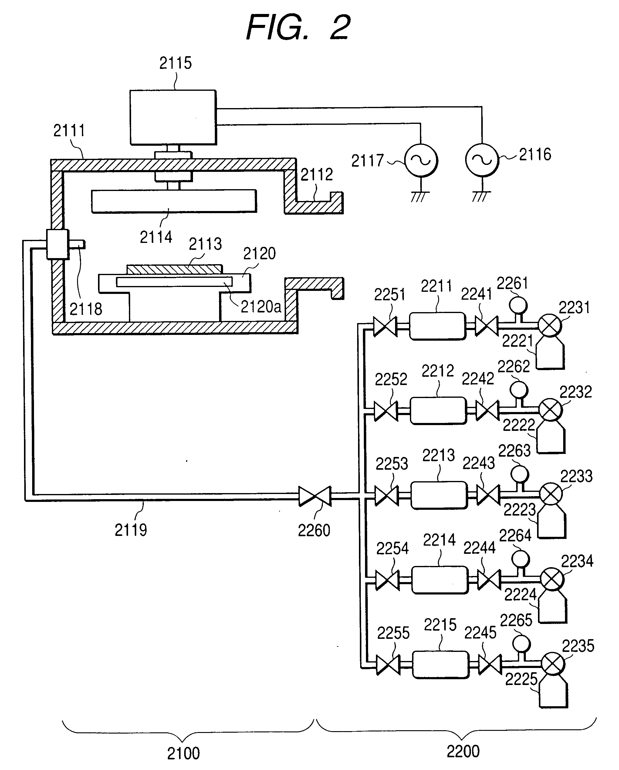
[0299] In this exemplary experiment, the apparatus shown in FIG. 2 was used to form the amorphous silicon deposited film on the conditions shown in Table 1. Polished glass (Corning #7059) of 1.times.1.5 inches (25.times.38 mm) was used as the substrate to be processed 2113, and this was installed as the 10 substrates of 1.times.1.5 inches (25.times.380 mm) arranged in the lengthwise direction at the center of the substrate stage 2120 of which length in the longer direction is 450 mm. The high-frequency power electrode 2114 is an alumina-sprayed stainless bar of which diameter is 10 mm and length is 500 mm, which was placed in parallel with the substrate 2113 at a distance of 60 mm therefrom.

[0300] The high-frequency power supplies 2116 and 2117 are comprised of a signal generator and amplifier respectively, and have a constitution capable of changing the oscillation frequencies. The amplifier of a first high-frequency power supply 2116 was adjusted to ...

exemplary experiment 2

[0313] (Exemplary Experiment 2)

[0314] In this exemplary experiment, the apparatus shown in FIG. 2 was used to form a hydrogenated amorphous silicon carbide film. The, placement of the substrates 2113, the high-frequency power electrode 2114 and so on was the same as the exemplary experiment 1.

[0315] For the high-frequency power supplies 2116 and 2117, those comprised of the signal generator and the amplifier capable of changing the frequencies were used just as in the exemplary experiment 1, and the oscillation frequencies thereof were variously changed to conduct this exemplary experiment.

[0316] In this exemplary experiment, the total power of the first high-frequency power supplied from the first high-frequency power supply 2116 and the second high-frequency power supplied from the second high-frequency power supply 2117 was 400 W, and the ratio of the second high-frequency power to the total power was 0.4. As for the frequencies, the frequency f1 of the first high-frequency power...

exemplary experiment 3

[0325] (Exemplary Experiment 3)

[0326] In this exemplary experiment, the apparatus shown in FIG. 2 was used to form the amorphous silicon deposited film. The placement of the substrates 2113, the high-frequency power electrode 2114 and so on was the same as the exemplary experiment 1.

[0327] In this exemplary experiment, the experiment was performed by fixing the oscillation frequency f1 of the first high-frequency power supply 2116 at 100 MHz and variously changing the oscillation frequency f2 of the second high-frequency power supply 2117. For the high-frequency power supplies 2116 and 2117, those comprised of the signal generator and the amplifier capable of changing the frequencies were used just as in the exemplary experiment 1, and adjustments were made to the amplifier and the matching box 2115 each time the oscillation frequency f2 of the second high-frequency power supply 2117 was changed.

[0328] In this exemplary experiment, the total power of the first high-frequency power s...


PUM

PropertyMeasurementUnit
frequenciesaaaaaaaaaa

Abstract

A vacuum processing method including placing an article to be processed in a reaction container and simultaneously supplying at least two high-frequency powers having different frequencies to the same high-frequency electrode to generate plasma in the reaction container by the high-frequency powers introduced into the reaction container from the high-frequency electrode. The frequencies and power values of the at least two high-frequency powers supplied satisfy a required relationship.

Description

[0001] 1. Field of the Invention[0002] The present invention relates to a vacuum processing method, a vacuum processing apparatus, a semiconductor device manufacturing method and a semiconductor device, using a high frequency power, which is used for forming a deposited film, etching and so on in semiconductor devices, electrophotographic photosensitive members, image input line sensors, photographing devices, photovoltaic devices and so on.[0003] 2. Related Background Art[0004] As for vacuum processing methods used when creating semiconductor devices, electrophotographic photosensitive members, image input line sensors, photographing devices, photovoltaic devices, other various electronic elements, optical elements and so on, many methods such as a vacuum evaporation method, a sputtering method, an ion plating method, a thermal CVD method, an photo-chemical vapor deposition method and a plasma CVD method are known, and apparatuses therefor are put into practice. Among others, a pla...

Claims


Application Information

Patent Timeline
Patent Type & Authority Applications(United States)
IPC IPC(8): H05H1/46C23C16/505G03G5/08G03G5/082H01J37/32H01L21/205
CPCG03G5/08278H01J37/32082H01J37/32568H01J37/32174H01J37/32183H01J37/32165
Inventor AOKI, MAKOTOSHIRASUNA, TOSHIYASUNIINO, HIROAKIAKIYAMA, KAZUYOSHIMURAYAMA, HITOSHITSUCHIDA, SHINJITAZAWA, DAISUKEABE, YUKIHIRO
Owner CANON KK
Why Eureka
Try Eureka