Circuit arrangement and method for phase modulation in a backscattering transponder

a backscattering transponder and circuit arrangement technology, applied in logic circuit coupling/interface arrangement, near-field system using receivers, instruments, etc., can solve the problems of significantly more complex and expensive controllable voltage sources having variable voltage outputs

Active Publication Date: 2004-12-23
ATMEL CORP +1
View PDF23 Cites 35 Cited by
  • Summary
  • Abstract
  • Description
  • Claims
  • Application Information

AI Technical Summary

Problems solved by technology

Such a controllable voltage source having a variable voltage output is significantly more complex and more co

Method used


Image

  • Circuit arrangement and method for phase modulation in a backscattering transponder
  • Circuit arrangement and method for phase modulation in a backscattering transponder

Examples


Embodiment Construction

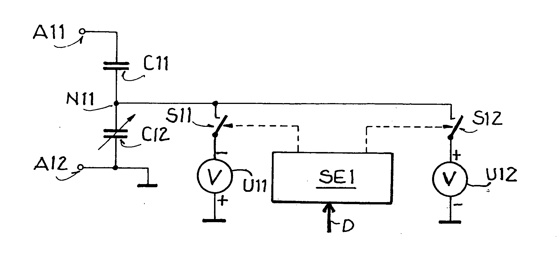
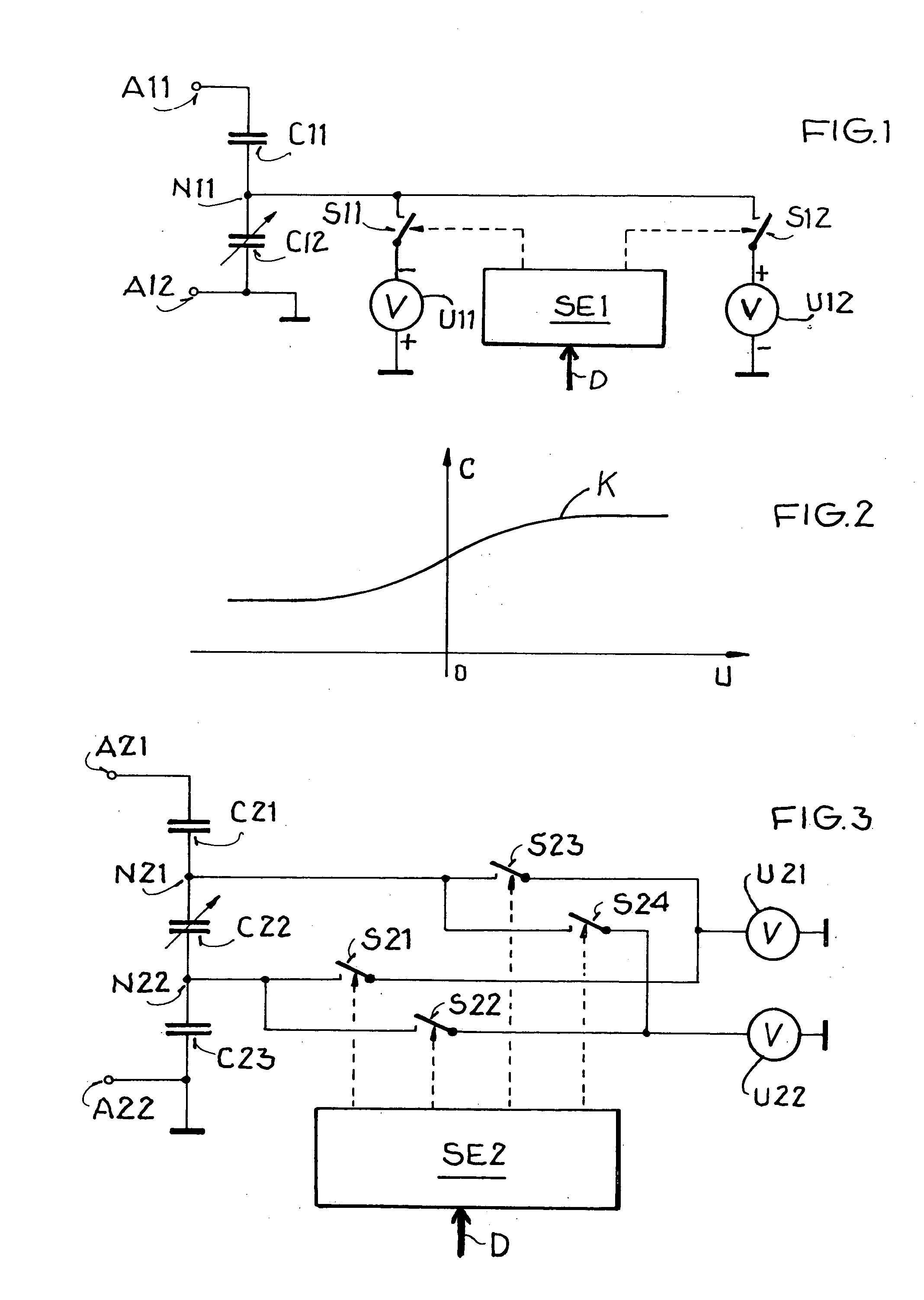
[0026] The circuit arrangement for phase modulation in a backscattering transponder as shown in FIG. 1 is a portion of an input circuit of the transponder, the rest of which is not shown. The inventive circuit arrangement comprises a capacitor C11 and a CMOS varactor C12 connected in series between two antenna terminals A11 and A12, a first voltage source U11 that is selectively connectable via a switching device S11 to a terminal N11 of the varactor C12 (e.g. the terminal N11 between the varactor C12 and the capacitor C11), and a second voltage source U12 that is selectively connectable via a second switching device S12 to the varactor terminal N11. Each of the switching devices S11 and S12 is preferably embodied as a high impedance CMOS switch. The circuit arrangement further comprises a control unit SE1 that is connected to and controls the switching devices S11 and S12.

[0027] The switching devices S11 and S12 together form a switching arrangement. The voltage sources U11 and U12...


PUM


Abstract

A circuit arrangement for phase modulation in an input circuit of a backscattering transponder includes a varactor and at least one capacitor connected in series between two antenna terminals, and at least two voltage sources selectively connected through at least two switches to at least one terminal of the varactor. A control unit selectively opens and closes the switches in response to the data to be phase-modulated onto the backscattered signal. By selectively connecting the different voltage values of the respective voltage sources to the varactor terminal(s) through the switches, the capacitance of the varactor and correspondingly the input impedance of the input circuit are thereby varied, so as to provide respective different phase positions of the phase modulation.

Description

[0001] This application is related to copending U.S. application Ser. Nos. 10 / 753,849 and 10 / 753,859, both filed Jan. 7, 2004, the entire disclosures of which are incorporated herein by reference. This application is further related to the US application entitled "Circuit Arrangement With Simplified Input Circuit For Phase Modulation In A Backscattering Transponder" by U. Friedrich and M. Fischer, being filed (under Docket No. 4671) on May 26, 2004, the entire disclosure of which is incorporated herein by reference.PRIORITY CLAIM[0002] This application is based on and claims the priority under 35 U.S.C. .sctn.119 of German Patent Application 103 25 396.3, filed on May 28, 2003, the entire disclosure of which is incorporated herein by reference.[0003] The invention relates to a circuit arrangement as well as a method for producing a phase modulation in a backscattering transponder having a varactor in an input circuit thereof.BACKGROUND INFORMATION[0004] There are various known syste...

Claims


Application Information

Patent Timeline
IPC IPC(8): H03K19/0175G06K19/07H01Q3/26H03C3/20H04B1/59H04B5/00H04B5/02
CPCG06K19/0723H04B5/0012H04B5/0068
Inventor FISCHER, MARTINFRIEDRICH, ULRICHKARTHAUS, UDO
Owner ATMEL CORP
Why Eureka
Try Eureka