Light receiving element and light receiving device incorporating circuit and optical disc drive

a light receiving device and circuit technology, applied in the direction of integrated optical head arrangements, record information storage, instruments, etc., can solve the problems of deterioration of light receiving device sensitivity, increased semiconductor layer, and deterioration of light receiving device response, so as to achieve excellent sensitivity and high response speed

Inactive Publication Date: 2005-01-06
SHARP KK
View PDF6 Cites 14 Cited by
  • Summary
  • Abstract
  • Description
  • Claims
  • Application Information

AI Technical Summary

Benefits of technology

According to the above configuration, although the thickness of the second conductivity type semiconductor layer is larger than the absorption length of incident light to the semiconductor layer, and a junction between the first conductivity type semiconductor layer and the second conductivity type semiconductor layer is placed at a relatively deep position, the impurity concentration in the vicinity of the surface of the second conductivity type semiconductor layer is not smaller than 1E17 cm−3 and not larger than 1E19 cm3. Consequently, in the vicinity of the surface of the second conductivity type semiconductor layer, recombination of carriers is effectively reduced, resulting in enhanced sensitivity of the light receiving device. Here, if the impurity concentration in the vicinity of the surface of the second conductivity type semiconductor layer is smaller than 1E17 cm−3, the resistance of the semiconductor layer is increased and therefore the response of the light receiving device is deteriorated. If the impurity concentration in the vicinity of the surface of the second conductivity type semiconductor layer is larger than 1E19 cm−3, recombination of carriers in the vicinity of the surface of the semiconductor layer is increased, thereby causing deterioration of the sensitivity of the light receiving device.
According to the above configuration, the light receiving device or the light receiving unit incorporating a circuit having excellent sensitivity and high response speed is used, thus, an optical disk drive particularly suitable for read and write access to a mass storage optical disk with use of light with a short wavelength is provided.

Problems solved by technology

Here, if the impurity concentration in the vicinity of the surface of the second conductivity type semiconductor layer is smaller than 1E17 cm−3, the resistance of the semiconductor layer is increased and therefore the response of the light receiving device is deteriorated.
If the impurity concentration in the vicinity of the surface of the second conductivity type semiconductor layer is larger than 1E19 cm−3, recombination of carriers in the vicinity of the surface of the semiconductor layer is increased, thereby causing deterioration of the sensitivity of the light receiving device.

Method used


Image

  • Light receiving element and light receiving device incorporating circuit and optical disc drive
  • Light receiving element and light receiving device incorporating circuit and optical disc drive
  • Light receiving element and light receiving device incorporating circuit and optical disc drive

Examples


first embodiment

(FIRST EMBODIMENT)

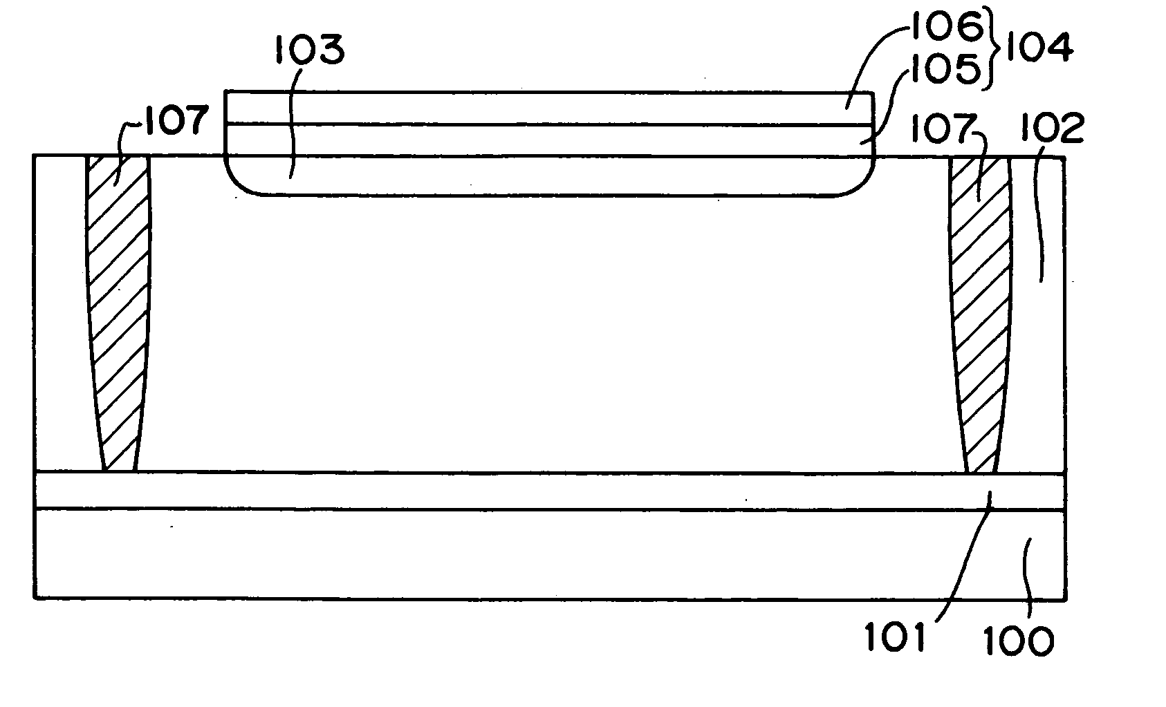
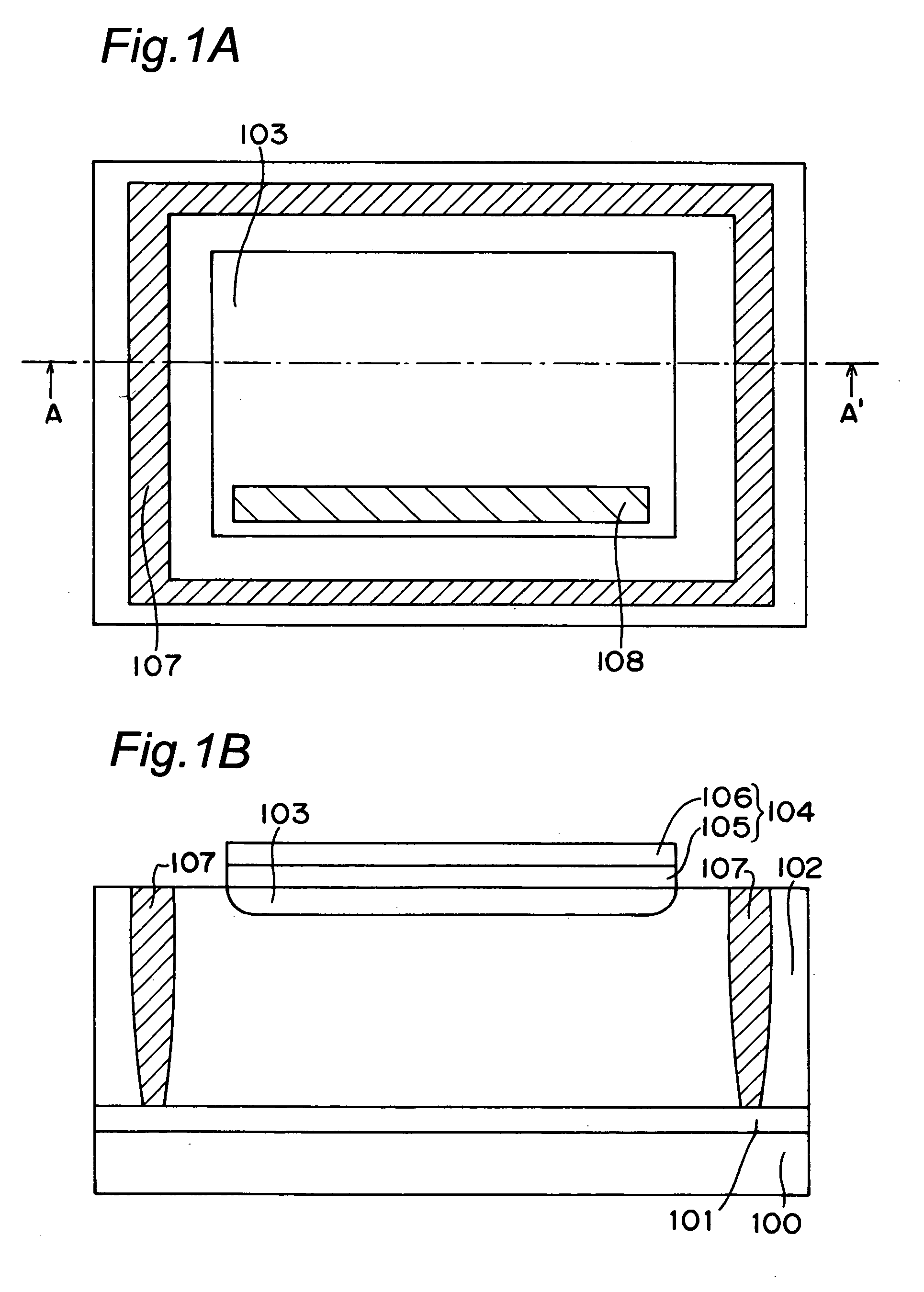
FIG. 1A is a plan view showing a light receiving device in a first embodiment of the present invention, while FIG. 1B is a cross sectional view taken along the line and shown by arrows A-A′ in FIG. 1A. It is noted that in the present embodiment, multilevel interconnections and interlayer films formed after the step for processing metal interconnections are deleted.

As shown in FIG. 1B, the light receiving device has a P type diffusion layer 101 with impurity concentration of about 1E18 cm−3 and a thickness of about 1 μm on a P type silicon substrate 100, and on top surface of the P type diffusion layer 101, has a P type semiconductor layer 102 as a first conductivity type semiconductor layer with impurity concentration of 1E13 cm−3 to 1E15 cm−3 and a thickness of about 10 μm to 20 μm. In the vicinity of the surface of the P type semiconductor layer 102, there is formed an N type diffusion layer (cathode) 103 as a second conductivity type semiconductor layer servin...

second embodiment

(SECOND EMBODIMENT)

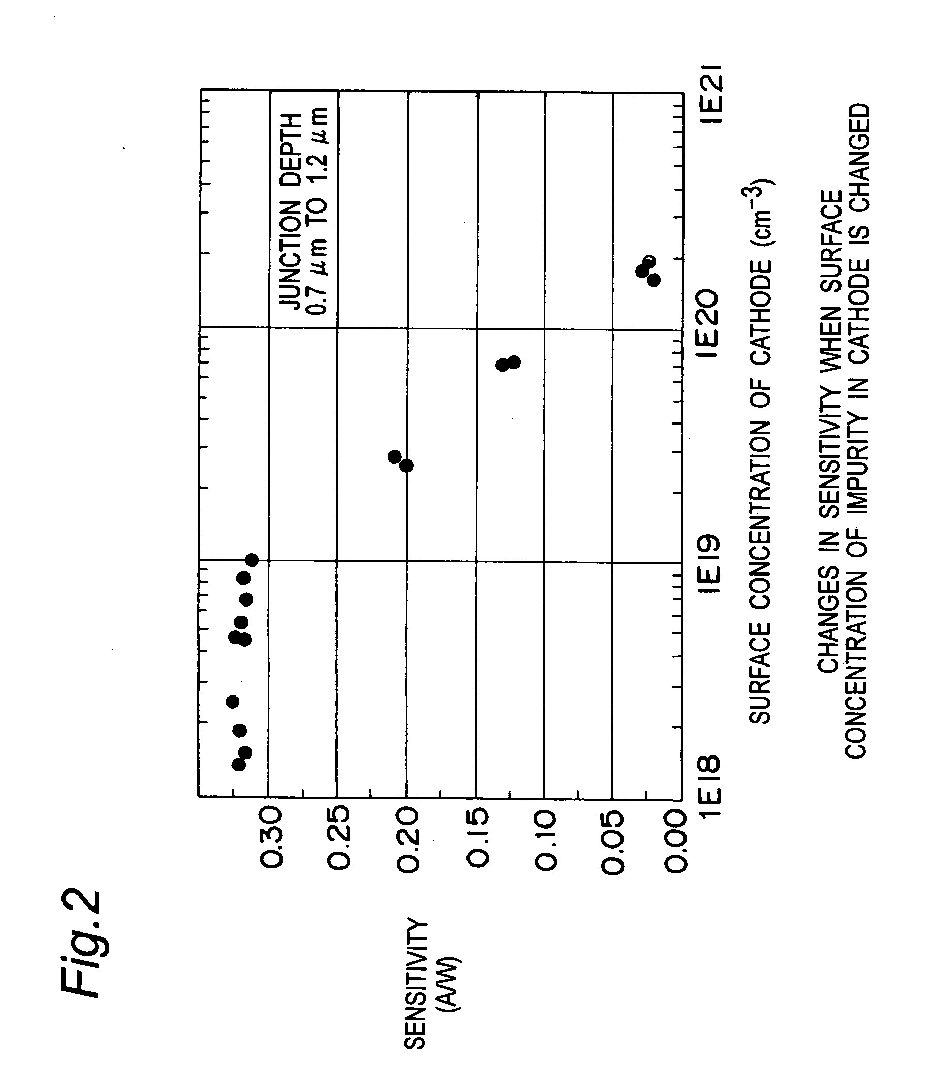
FIG. 7 is a graph showing an impurity concentration profile of an N type diffusion layer as a second conductivity type semiconductor layer and a P type semiconductor layer as a first conductivity type semiconductor layer of a light receiving device in the second embodiment of the present invention. The N type diffusion layer forms a light receiving part while the P type semiconductor layer contacts the N type diffusion layer. In the N type diffusion layer that forms the light receiving part, As (arsenic) is used as an impurity. The concentration profile shown in FIG. 7 is formed by detecting the impurity concentration with SIMS (Secondary Ion Mass Spectrometer).

The light receiving device in the second embodiment has the same configuration as the light receiving device in the first embodiment except the point that the impurity of the N type diffusion is As. In this embodiment, description is made with use of the reference numerals identical to those used for the ...

third embodiment

(THIRD EMBODIMENT)

FIG. 10 is a cross sectional view showing a light receiving device in a third embodiment of the present invention. It is noted that in the present embodiment, multilevel interconnections and interlayer films formed after the step for processing metal interconnections are deleted.

The light receiving device of the present embodiment has a P type diffusion layer 201 with impurity concentration of about 1E18 cm−3 and a thickness of about 1 μm formed on a P type silicon substrate 200, and has a P type semiconductor layer 202 as a first conductivity type semiconductor layer with impurity concentration of about 1E13 cm−3 to 1E15 cm−3 and a thickness of about 10 μm to 20 μm formed on the P type diffusion layer 201. Reference numeral 203 is an N type semiconductor layer. Reference numeral 204 is an N type diffusion layer as a second conductivity type semiconductor layer with an impurity diffused for reducing resistance, and the impurity concentration in the vicinity of th...


PUM

PropertyMeasurementUnit
absorption lengthaaaaaaaaaa
thicknessaaaaaaaaaa
conductivityaaaaaaaaaa

Abstract

A light receiving device includes a P type diffusion layer (101), a P type semiconductor layer (102), an N type diffusion layer (103) serving as a light receiving part, and a light transmitting film (104), all formed on a p type silicon substrate (100). The N type diffusion layer (103) has a thickness of 0.8 μm to 1.0 μm which is larger than an absorption length of incident light having wavelength of 400 nm, and such a concentration profile that a impurity concentration is not higher than 1E19 cm−3 on a surface and has a peak in a vicinity of the surface. Since recombination of carriers generated by the incident light is prevented in the vicinity of the surface of the N type diffusion layer (103), sensitivity of the light receiving device is enhanced and response speed is increased by the low-resistance N type diffusion layer (103) having a larger junction depth.

Description

This Nonprovisional application claims priority under 35 U.S.C. §119(a) on Patent Application No. P2001-394221 filed in Japan on Dec. 26, 2001, the entire contents of which are hereby incorporated by reference. TECHNICAL FIELD The present invention relates to a light receiving device, a light receiving unit incorporating a circuit, and an optical disk drive. BACKGROUND ART Conventionally, optical disk drives for optical disks such as CDs (Compact Discs) and DVDs (Digital Versatile Disks) are provided with an optical pickup. The optical pickup includes a semiconductor laser device for emitting a light beam to be radiated to an optical disk and a light receiving device for receiving a reflected light beam radiated to and reflected by the optical disk. In recent years, higher-density DVDs are being vigorously developed, which demands for processing large-volume data such as dynamic images and for higher read rates such as 12X. Since an amount of a data storage capacity of the optica...

Claims


Application Information

Patent Timeline
Patent Type & Authority Applications(United States)
IPC IPC(8): G11B7/12G11B7/123G11B7/13H01L27/14H01L31/0216H01L31/10H01L31/103
CPCG11B7/123G11B7/13H01L31/103H01L31/02161H01L27/14
Inventor HAYASHIDA, SHIGEKIMORIOKA, TATSUYATANI, YOSHIHIKOOHKUBO, ISAMUWADA, HIDEO
Owner SHARP KK
Why Eureka
Try Eureka