Gate driving circuit

Active Publication Date: 2005-01-06
DENSO CORP
View PDF7 Cites 31 Cited by
  • Summary
  • Abstract
  • Description
  • Claims
  • Application Information

AI Technical Summary

Benefits of technology

[0030] It is preferable that anti-parallel diodes are connected to or installed in the first and second control elements. In this case, at the resonance time after the ON-driving element is turned off, current can continue to flow in the reactor through the anti-parallel diode of the first control element even when both the first and second control elements are t

Problems solved by technology

However, such a driving target device has a drawback of an increased switching loss at the transit time when the ON/OFF state is switched (see FIG.
That is, in the adjustment method using the gate resistor as described above, there is a tradeoff between reduction of noise and reduction of switching loss (high-speed switching).
Thus, both of the noise and the switching loss cannot be reduced at the same time.
Accordingly, the related-art device must be constructed by elements which operate at high speed to make the gate resistance value variable and also a high-precision sensor for detecting a high

Method used


Image

  • Gate driving circuit
  • Gate driving circuit
  • Gate driving circuit

Examples


first embodiment

[0062] (First Embodiment)

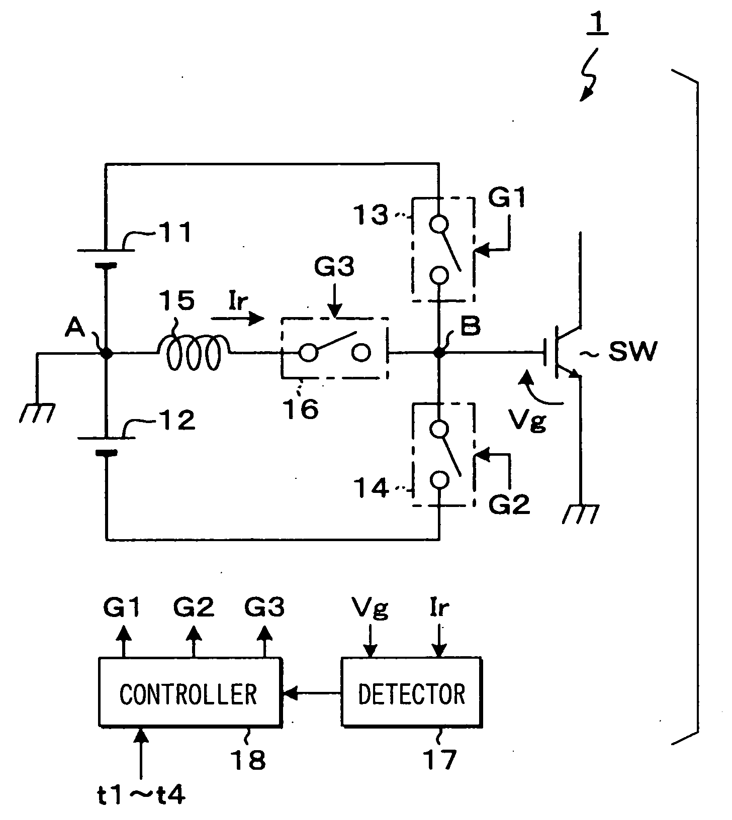
[0063]FIG. 1 is a circuit diagram showing the construction of a gate driving circuit according to a first embodiment for carrying out an ON / OFF driving operation of a driving target device which corresponds to a voltage driving type switching device. In this embodiment, IGBT (insulated gate bipolar transistor) is used as a driving target device SW. The reference potential of a gate voltage is set to emitter potential.

[0064] As shown in FIG. 1, a gate driving circuit 1 of this embodiment is equipped with a pair of DC power sources 11, 12 which are connected to each other in series, and the connection point between the DC power supply sources (hereinafter referred to as “power source intermediate point”) A is set as a reference potential.

[0065] The gate driving circuit 1 is further equipped with a driving element unit comprising a switching element (hereinafter referred to as “ON-driving element”) 13 through which a power supply passage for supplying a posit...

second embodiment

[0100] (Second Embodiment)

[0101] Next, a second embodiment according to the present invention will be described.

[0102] A gate driving circuit 1a of this embodiment is different from the gate driving circuit 1 of the first embodiment merely in a part of the construction, and the same constituent elements between the first and second embodiments are represented by the same reference numerals. Therefore, the descriptions on the same constituent elements are omitted, and only the difference in construction will be mainly described.

[0103] As shown in FIG. 7A, the gate driving circuit 1a of this embodiment uses anti-parallel diodes connected to or installed in the gate driving circuit 1a as an ON-driving element 13a and an OFF-driving element 14a. In the gate driving circuit 1a of this embodiment thus constructed, the same operation of the gate driving circuit 1 of the first embodiment is carried out except for the following case.

[0104] That is, if the gate voltage Vg exceeds the ON-vo...

third embodiment

[0106] (Third Embodiment)

[0107] Next, a third embodiment according to the present invention will be described.

[0108] A gate driving circuit 1b of this embodiment is different from the gate driving circuit 1 of the first embodiment merely in a part of the construction, and the same constituent elements between the first and third embodiments are represented by the same reference numerals. Therefore, the descriptions on the same constituent elements are omitted, and only the difference in construction will be mainly described.

[0109] As shown in FIG. 9, the gate driving circuit 1b of this embodiment has a construction achieved by deleting the auxiliary driving element 16 from the gate driving circuit 1 of the first embodiment, and a controller 18b is designed to execute the switching control processing to generate the gate signals G1, G2 to switch the ON-driving element 13 and the OFF-driving element 14 on the basis of the detection result of the detector 17 and the set times t3, t4....


PUM


Abstract

In a gate driving circuit, when a driving target device is turned on, an auxiliary driving element is turned on to form a closed circuit comprising a DC power source, a reactor, an auxiliary driving element and an OFF-driving element, and make reactor current flow in the direction from a power source intermediate point to an output point in advance. Just before the driving target device is turned on, the OFF-driving element is turned off to form a resonance circuit comprising the reactor, the auxiliary driving element and the gate capacitance, and make gate current (reactor current) flow so that the gate capacitance is charged by using resonance phenomenon of the resonance circuit.

Description

CROSS REFERENCE TO RELATED APPLICATIONS [0001] This application is based upon, claims the benefit of priority of, and incorporates by reference the contents of, Japanese Patent Application No. 2003-270430 filed on Jul. 2, 2003 and Japanese Patent Application No. 2004-106095 filed on Mar. 31, 2004. FIELD OF THE INVENTION [0002] The present invention relates to a gate driving circuit for a switching element. BACKGROUND OF THE INVENTION [0003] A conventional driving circuit for driving a voltage driving type semiconductor switching device such as FET, IGBT or the like includes a switching element (hereinafter referred to as “ON-driving element”) for applying an ON-voltage to the gate of a switching element to be driven (hereinafter referred to as “driving target device”) and a switching element (hereinafter referred to as “OFF-driving element”) for applying an OFF-voltage to the gate of the driving target device. [0004] This type of driving circuit controls an ON / OFF state of the drivi...

Claims


Application Information

Patent Timeline
IPC IPC(8): H02M1/08H03K17/0412H03K17/0416
CPCH02M1/08H03K17/04123H03K2217/009H03K17/04163H03K17/04166H03K17/04126
Inventor INOSHITA, RYOUSUKE
Owner DENSO CORP
Why Eureka
Try Eureka