Apparatus for forming a film and an electroluminescence device

a technology of electroluminescence device and film, which is applied in the direction of sports apparatus, organic semiconductor devices, skating, etc., can solve the problems of high production cost of light-emitting devices, low utilization efficiency of expensive el materials in the formation of el layers, and easy non-uniform film thickness in the central zon

Inactive Publication Date: 2005-01-13
SEMICON ENERGY LAB CO LTD
View PDF48 Cites 118 Cited by
  • Summary
  • Abstract
  • Description
  • Claims
  • Application Information

AI Technical Summary

Benefits of technology

[0013] The present invention provides a production apparatus equipped with a deposition apparatus, which is a production apparatus reducing production cost by increasing the utilization efficiency of EL materials and having excellent uniformity and throughput of EL layer deposition.
[0014] Further, the present invention also provides a production apparatus for efficient deposition of EL materials on substrates with a large surface area such as 320 mm×400 mm, 370 mm×470 mm, 550 mm×650 mm, 600 mm×720 mm, 680 mm×880 mm, 1000 mm×1200 mm, 1100 mm×1250 mm, and 1150 mm×1300 mm. Further, the present invention also provides a deposition apparatus for obtaining a uniform film thickness over the entire substrate surface even on a substrate with a large surface area.

Problems solved by technology

For this reason, the utilization efficiency of expensive EL materials in the formation of the EL layer was extremely low, about 1% or less, and the production cost of light-emitting devices was extremely high.
Further, a problem associated with substrates with a large surface area is that the film thickness can easily become nonuniform in the central zone and peripheral edges of the substrate.
Moreover, because the deposition apparatus has a structure with a rotating substrate, a limitation is placed on the deposition apparatuses designed for substrates with a large surface area.
In addition, if a substrate with a large surface area and a mask for deposition are rotated together after being brought into intimate contact with each other, there is a risk of the displacement occurring between the mask and the substrate.
As a result, the dimensional accuracy and positional accuracy decrease owing to the difference in thermal expansion coefficient between the mask and substrate.

Method used


Image

  • Apparatus for forming a film and an electroluminescence device
  • Apparatus for forming a film and an electroluminescence device
  • Apparatus for forming a film and an electroluminescence device

Examples


first embodiment

[0058] (First Embodiment Mode)

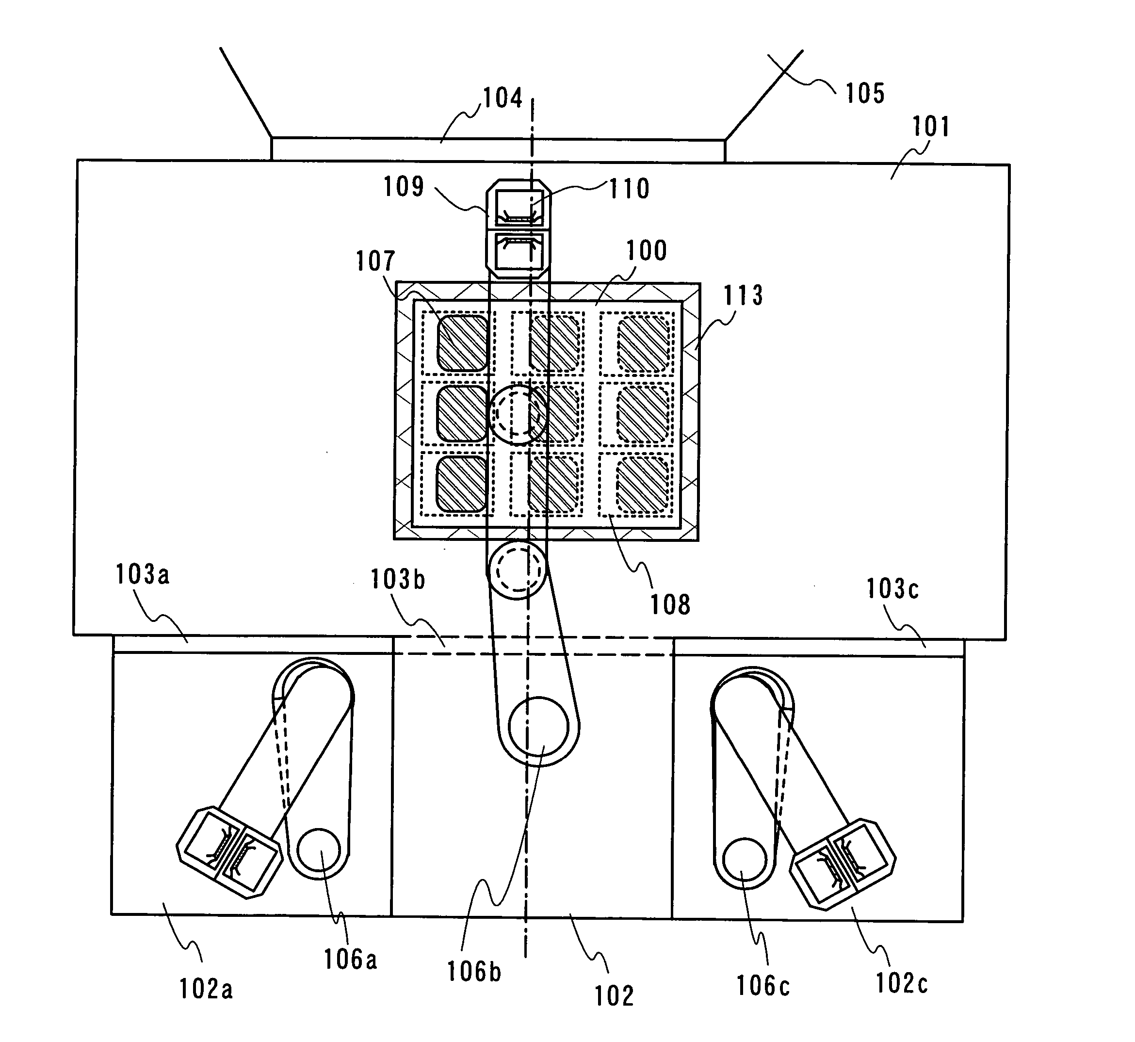
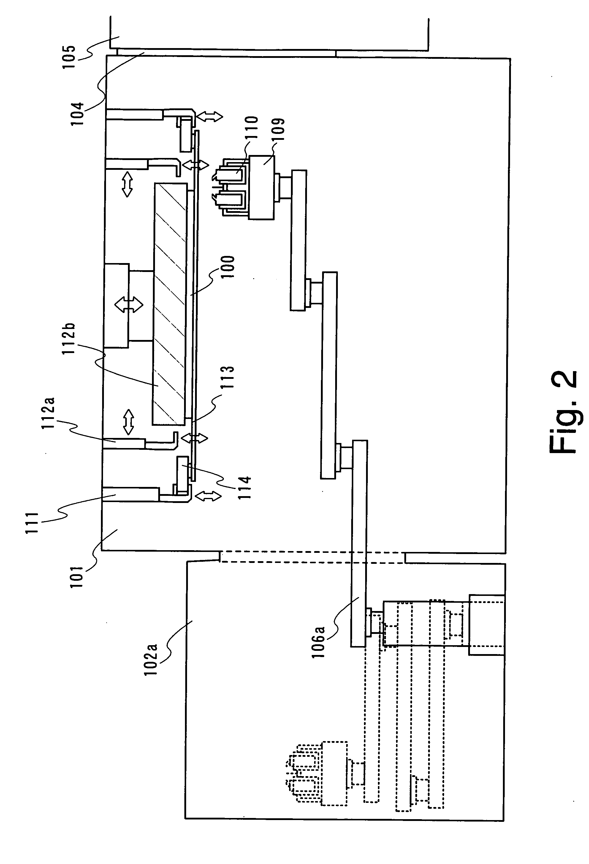
[0059]FIG. 1 shows an example of a top view of an evaporation device of the invention.

[0060] In FIG. 1, reference numeral 100 denotes a substrate; 101, a film formation chamber; 102a to 102c, installation chambers; 103a to 103c and 104, shutters; 105, a conveyance chamber; 106a to 106c, robot arms; 107, evaporated areas; 108, areas to be panels; 109, an evaporation holder, and 110, a container.

[0061] Note that an example in which nine areas to be panels 108 are designed on the substrate 100 is shown.

[0062] Although an example in which the shutters 103a to 103c and the installation chambers 106a to 106c are arranged in sideways is shown here, the arrangement is not specifically limited, and three robots may be arranged in one installation chamber.

[0063] In addition, a mask 113 is aligned in contact with the substrate 100, and RGB are separately coated by shifting one mask by a size of one pixel and performing alignment several times to perform evapor...

second embodiment

[0076] (Second Embodiment Mode)

[0077] Here, an example for performing seal dripping, seal drawing, or formation of auxiliary wiring with a droplet jet method, representatively, an ink jet method, using a device shown in FIG. 5 will be described.

[0078]FIG. 5A is a schematic perspective view showing an example of a structure of a linear droplet jet device. The linear droplet jet device shown in FIG. 5A has heads 306a to 306c and jets droplets from the heads 306a to 306c to thereby obtain a desired droplet pattern on a substrate 310. The linear droplet jet device can be applied to, other than a glass substrate with a desired size, a resin substrate represented by a plastic substrate, or a treated object such as a semiconductor wafer represented by silicon as the substrate 310.

[0079] In FIG. 5A, the substrate 310 is carried into a treatment chamber 515 from a carrying entrance 304, the substrate subjected to droplet jetting treatment is returned and carried out from the carrying entra...

third embodiment

[0101] (Third Embodiment Mode)

[0102] Here, a method of controlling deviation of an evaporation pattern is provided.

[0103] Usually, a TFT, a pixel electrode (an electrode to be an anode or a cathode of an electroluminescence element), and a partition wall (also called a bank) are formed according to a marker on a substrate. Thereafter, evaporation is applied to the substrate in which the TFT, the pixel electrode, and the partition wall (bank) are formed. In particular, if positions of the pixel electrode and a layer containing organic compounds deviate, a defect, for example, short circuit is caused.

[0104] In a mask for multiple forming, several masks adhere with each other in the same pattern. If accuracy of adhesion is poor, deviation occurs for each panel.

[0105] Thus, in the invention, a stepper exposure position is corrected on the basis of an evaporation pattern, which is obtained by applying evaporation to a dummy substrate using a mask, a TFT is manufactured on the basis of...


PUM

PropertyMeasurementUnit
distanceaaaaaaaaaa
space distanceaaaaaaaaaa

Abstract

A device having three evaporation sources and a unit for moving the respective evaporation sources in one chamber is used, whereby it becomes possible to increase efficiency of use of an evaporation material. Consequently, manufacturing cost can be reduced, and a uniform thickness can be obtained over an entire surface of a substrate even in the case in which a large area substrate is used.

Description

TECHNICAL FIELD TO WHICH THE INVENTION BELONGS [0001] The present invention relates to a film forming apparatus employed for forming a film of a material capable of forming a film by deposition (referred to herein below as a deposition material) and a production apparatus comprising such a film forming apparatus. In particular, the present invention relates to an evaporation apparatus in which a film is formed by evaporating a deposition material from a deposition source provided opposite to a substrate. Besides, the present invention also relates to an electroluminescence device and method of manufacturing thereof. [0002] 1. Prior Art [0003] Light-emitting elements using organic compounds featuring small thickness and weight, fast response, DC low-voltage drive, and the like, as light-emitting substances have been expected to find application in flat panel displays of the next generation. In particular, display devices in which light emitting elements are disposed as a matrix have ...

Claims


Application Information

Patent Timeline
Patent Type & Authority Applications(United States)
IPC IPC(8): C23C14/00H05B33/10C23C14/12C23C14/24C23C16/00H01L51/00H01L51/40H01L51/50H01L51/56H05B33/04H05B33/14
CPCC23C14/12C23C14/24H01L51/001H05B33/10H01L51/56H01L2251/5323H01L51/5246H10K59/12H10K71/164H10K50/8426H10K50/8445H10K2102/3031H10K71/00A63C17/22A63C17/06
Inventor YAMAZAKI, SHUNPEIKUWABARA, HIDEAKI
Owner SEMICON ENERGY LAB CO LTD
Why Eureka
Try Eureka