EUV condenser with non-imaging optics

Inactive Publication Date: 2005-01-13
ASML HLDG NV
View PDF10 Cites 10 Cited by
  • Summary
  • Abstract
  • Description
  • Claims
  • Application Information

AI Technical Summary

Benefits of technology

It is an advantage of the present invention that it is an efficient c-condenser for the desired wavelength.
It is a further advantage of the present invention that it is relatively compact.

Problems solved by technology

As the element or feature size desired to be imaged on the photosensitive substrate becomes ever smaller, technical problems often arise.
One of these problems is illuminating the reticle or mask so that its image can be projected onto the photosensitive substrate.
While the projection optic system disclosed therein can achieve a working resolution of 0.03 microns, there are few illumination sources or illumination systems that can provide the required illumination properties for projecting the image of the reticle or mask onto the photosensitive substrate.
However, these prior illumination systems may not provide the desired illumination and are relatively complicated.
Additionally, many of these systems are relatively large, having many surfaces resulting in loss of energy.
Some are also difficult: to align and may require adjustment.

Method used


Image

  • EUV condenser with non-imaging optics
  • EUV condenser with non-imaging optics
  • EUV condenser with non-imaging optics

Examples


Embodiment Construction

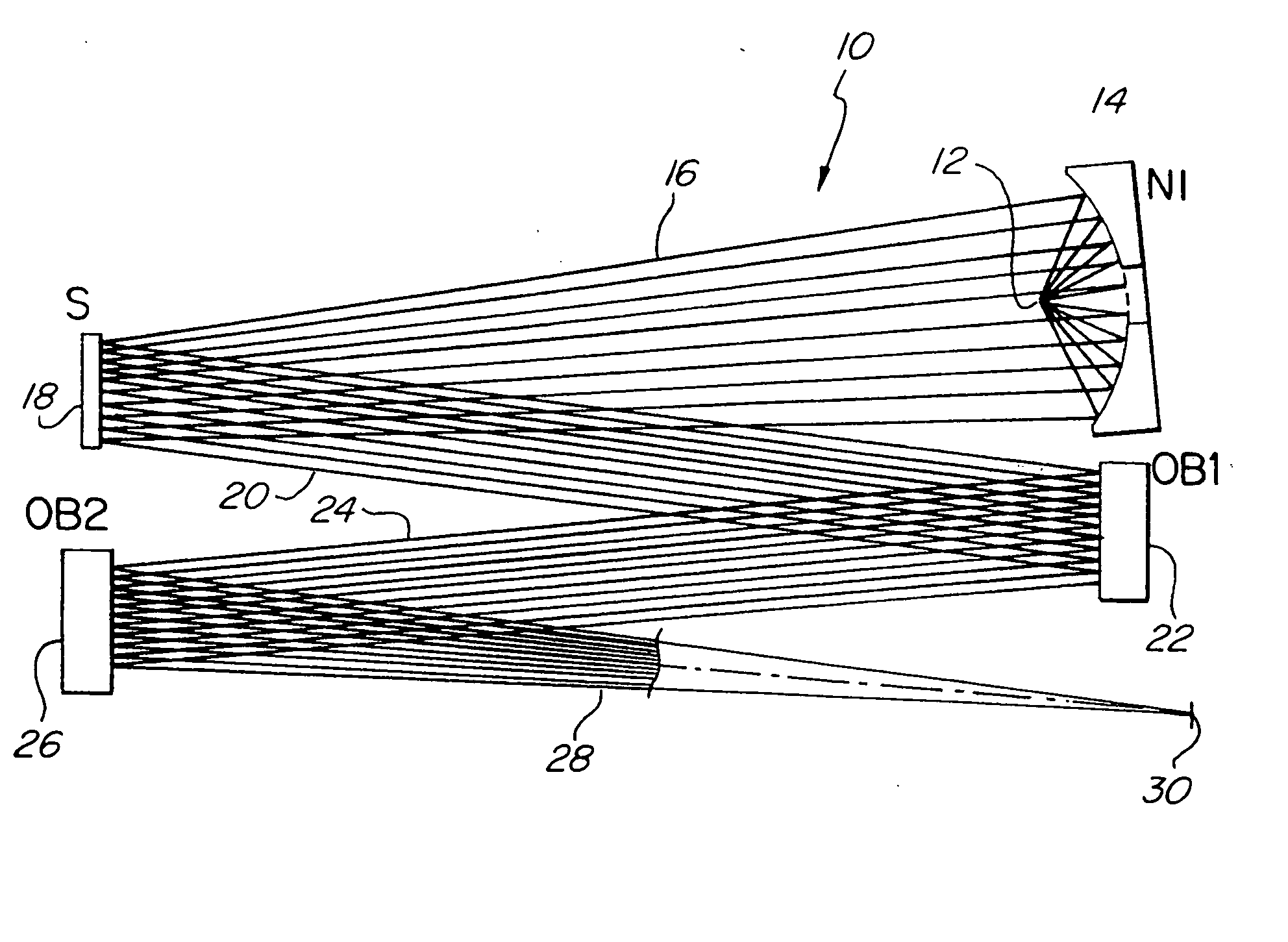
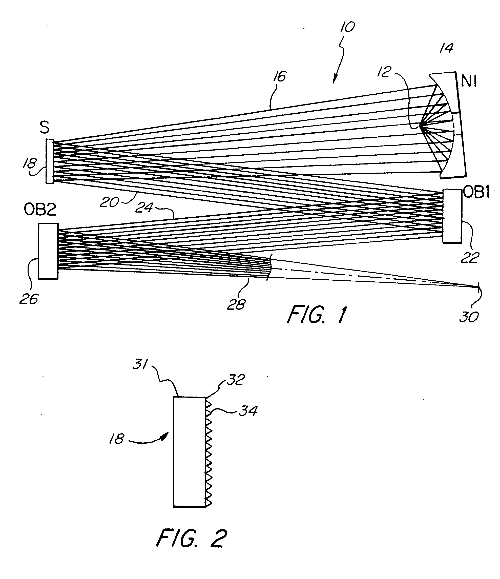
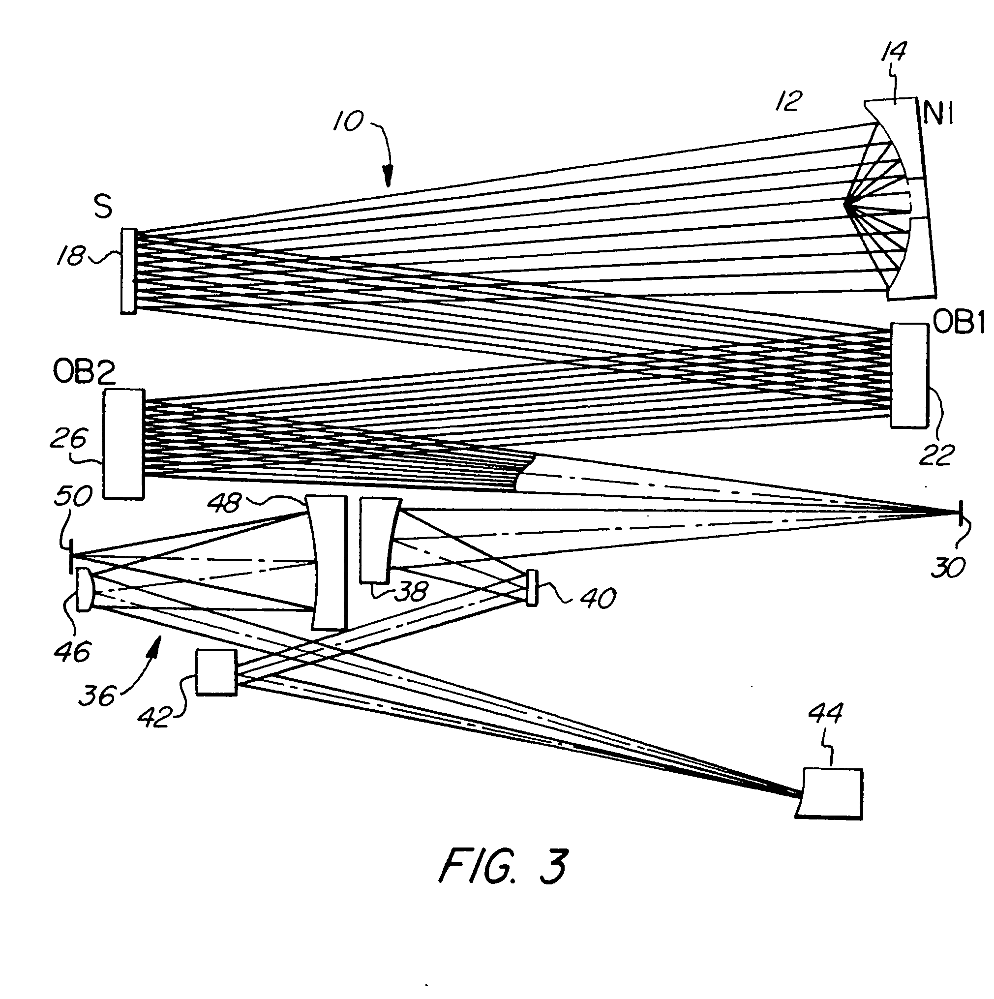
FIG. 1 schematically illustrates the illumination system 10 of the present invention utilizing non-imaging optics. An extreme ultrawide, radiation, EUV, source 12, which may be a laser plasma source, a capillary discharge tube or synchrotron, provides electromagnetic radiation in the extreme ultraviolet to a non-imaging optic element 14. The collector or first non-imaging optic element 14 collects the electromagnetic radiation from the source and creates a desired or predetermined radiance distribution in the pupil of the illumination system 10. The radiance distribution may be uniform, annular, quadruple or other known or desired radiance distribution. Various radiance distributions have known desirable properties for imaging different patterns onto a photosensitive substrate. Coatings having a graded thickness profile may be place on the first non-Imaging optic element 14 to improve reflectivity. The electromagnetic radiation reflected from the first non-imaging optic element 14 i...


PUM

PropertyMeasurementUnit
Lengthaaaaaaaaaa
Sizeaaaaaaaaaa
Wavelengthaaaaaaaaaa

Abstract

An illumination system and condenser for use in photolithography in the extreme ultraviolet wavelength region has a first non-imaging optic element collecting electromagnetic radiation from a source and creates a desired radiance distribution. A second non-imaging optic element receives the electromagnetic radiation from the first non-imaging optic element and redirects and images the electromagnetic radiation. The electromagnetic radiation from the second non-imaging optic element is suitable for being received by other conventional optical surfaces to provide a desired radiance distribution with a desired angular distribution and desired shape. Facets are used to provide the desired illumination over the desired illumination field. Reflective facets may be placed on the second non-imaging optic, which can reduce the number of mirrors and increase efficiency. The condenser and illumination system are used in combination with a projection optic to project the image of a reticle or mask onto a photosensitive substrate, such as a semiconductor wafer. The condenser of the present invention provides an efficient condenser in a compact package and provides desirable illumination properties for imaging relatively small feature sizes of less than 0.13 microns.

Description

FIELD OF THE INVENTION The present invention relates generally to a condenser and illumination systems for projecting the image of a reticle onto a photosensitive substrate as used in photolithography in semiconductor manufacturing, and more particularly to a condenser suitable for use in the extreme ultraviolet or soft X-ray wavelengths having non-imaging optics forming a desired radiance and desired angular distribution. BACKGROUND OF THE INVENTION Photolithography is often used in the manufacture of many devices and in particular, electronic or semiconductor devices. In a photolithographic process, the image of a reticle or mask is projected onto a photosensitive substrate. As the element or feature size desired to be imaged on the photosensitive substrate becomes ever smaller, technical problems often arise. One of these problems is illuminating the reticle or mask so that its image can be projected onto the photosensitive substrate. As the element or feature size of semicondu...

Claims


Application Information

Patent Timeline
IPC IPC(8): G02B17/06G02B19/00G03F7/20H01L21/027
CPCG03F7/70075G03F7/70233G03F7/702G03F7/70108Y10T428/3154
Inventor MCGUIRE, JAMES P. JR.
Owner ASML HLDG NV
Why Eureka
Try Eureka