Apparatus and method for optical modulation

a technology of optical modulation and apparatus, applied in the field of apparatus for optical modulation and optical modulation method, can solve the problems of xpm (cross phase modulation) becoming a problem, affecting the transmission characteristics of high-speed drive circuits, and reducing the breakdown voltage, so as to achieve the effect of reducing degradation and large frequency bandwidth

Inactive Publication Date: 2005-01-20
KK TOSHIBA
View PDF2 Cites 10 Cited by
  • Summary
  • Abstract
  • Description
  • Claims
  • Application Information

AI Technical Summary

Benefits of technology

[0009] An object of the present invention is to provide an apparatus for optical modulation and a method of optical modulation which enable the output of an RZ-coded optical signal as an optical transmission signal to suppress degradation due to XPM and eliminate the need for an optical modulator to have a large frequency bandwidth.
[0012] In this optical modulator, the phase modulator drives light with an NRZI-coded drive signal to generate an NRZI-coded optical signal which is supplied to the intensity modulator. The intensity modulator is prevented from outputting an intensity-modulated optical signal when the received phase-modulated NRZI-coded optical signal is not varied so that an optical signal output by the intensity modulator is an RZ-coded optical signal. The intensity modulator can thus output an RZ-coded optical signal as an optical signal sent out to an optical transmission path, preventing degradation due to XPM. The phase modulator is driven by an NRZI-coded drive signal, so that a frequency bandwidth required for the phase modulator is only approximately half the bit rate of a data signal by Nyquist theorem. The phase modulator thus does not need to have a large frequency bandwidth.

Problems solved by technology

The increase in optical power supplied to an optical fiber, however, results in an increase in the nonlinear optical effects of the optical fiber on the transmission characteristics.
Especially in dense wavelength division multiplexing transmissions, the effect of XPM (Cross Phase Modulation) becomes a problem.
However, high-speed drive circuits tend to use smaller-sized transistors and have lower breakdown voltage.
This results in technical difficulties in configuring a high-speed high-voltage-output drive circuit.

Method used


Image

  • Apparatus and method for optical modulation
  • Apparatus and method for optical modulation
  • Apparatus and method for optical modulation

Examples


first embodiment

[0028] [First Embodiment]

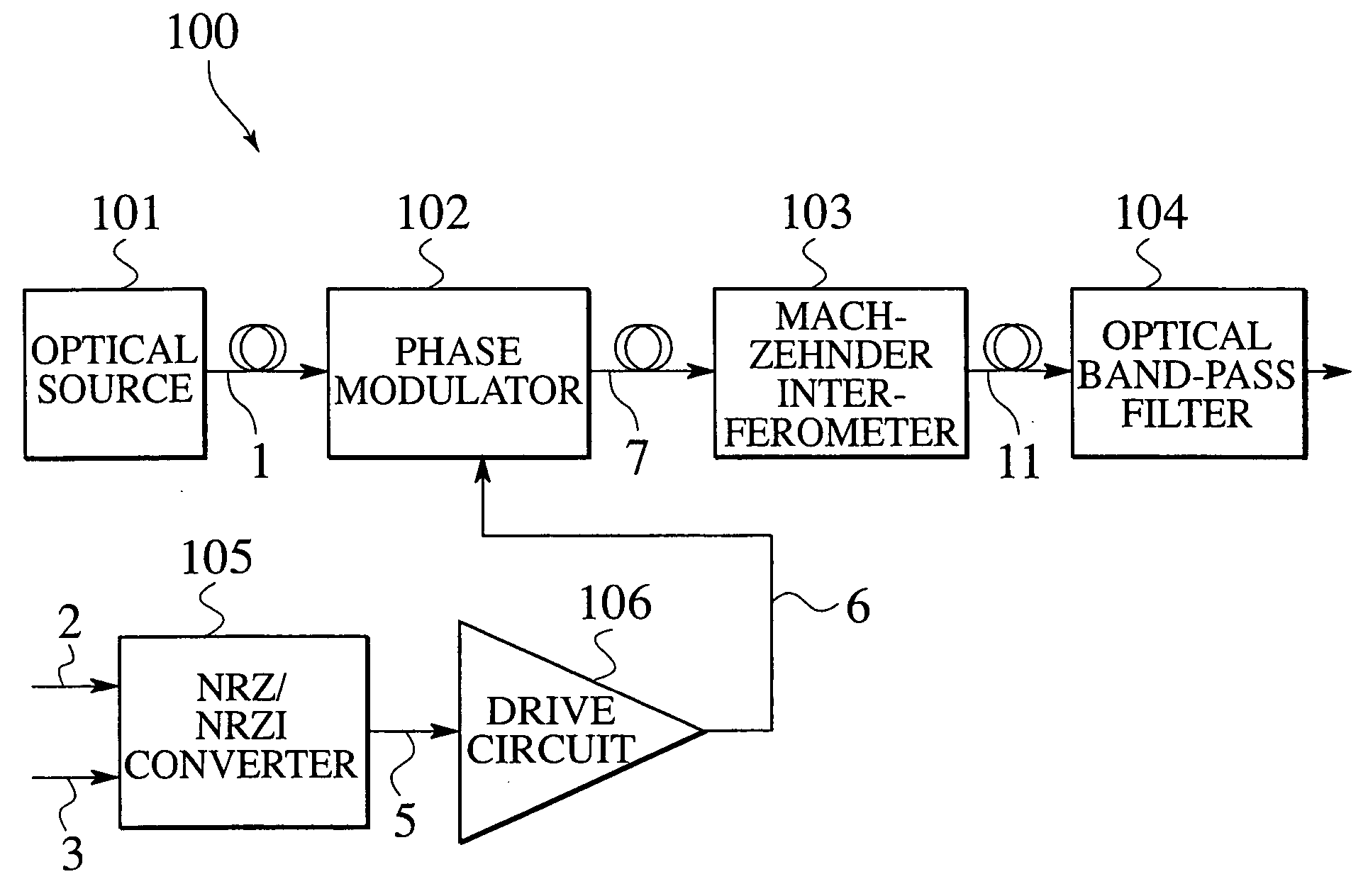
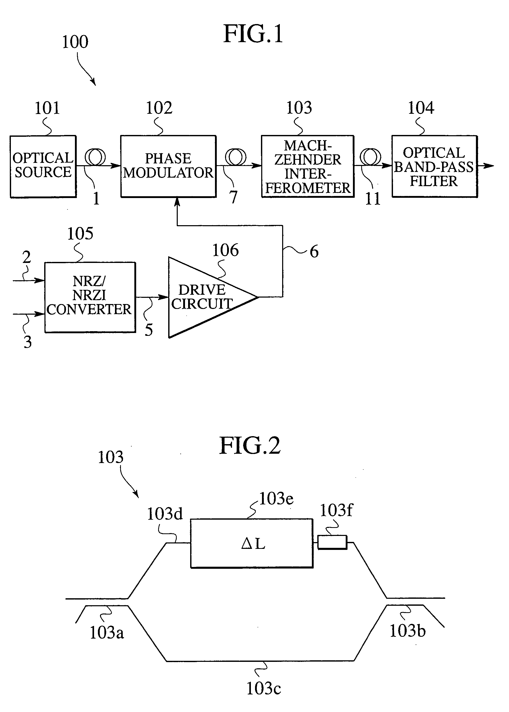
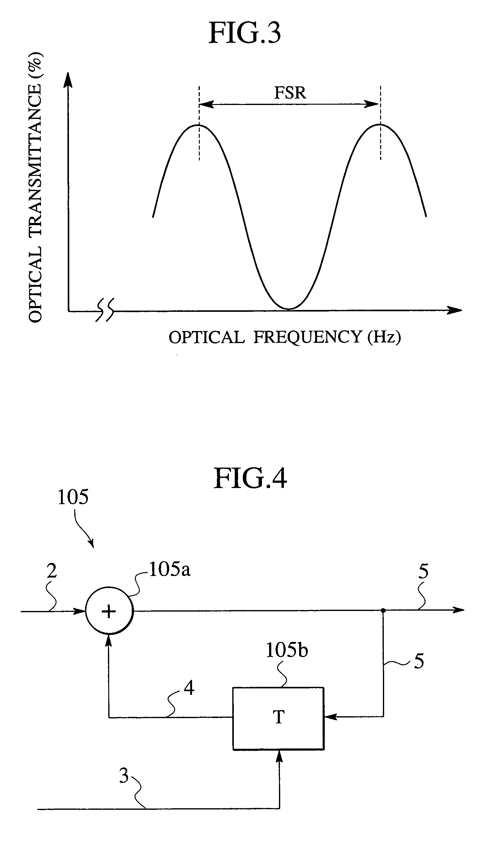
[0029]FIG. 1 is a block diagram illustrating the configuration of an optical modulator 100 according to a first embodiment. The optical modulator 100 includes an optical source 101, a phase modulator 102, a Mach-Zehnder interferometer 103, an optical band-pass filter 104, an NRZ / NRZI converter 105, and a drive circuit 106.

[0030] The optical source 101 outputs light 1 to an input of the phase modulator 102. The optical source 101 may be, e.g., a semiconductor laser which oscillates in a single longitudinal mode. The phase modulator 102 drives the light 1 received from the optical source 101 with an NRZI-coded drive signal 6 for phase modulation. The phase modulator 102 is driven by the drive signal 6 fed from the drive circuit 106 to the phase modulator 102 for phase modulation. The phase modulator 102 supplies an NRZI-coded optical signal 7 obtained by the phase modulation to an input of the Mach-Zehnder interferometer 103.

[0031] The Mach-Zehnder interfero...

second embodiment

[0078] [Second Embodiment]

[0079]FIG. 10 is a block diagram illustrating the configuration of an optical modulator 200 according to a second embodiment. The optical modulator 200 includes an optical source 201, a phase modulator 202, a Mach-Zehnder interferometer 203, an optical band-pass filter 204, an NRZ-NRZI converter 205, a drive circuit 206, an O / E converter 207, and a temperature control circuit 208. In FIG. 10, the optical source 201, phase modulator 202, optical band-pass filter 204, NRZ-NRZI converter 205 and drive circuit 206 are substantially identical to the optical source 101, phase modulator 102, optical band-pass filter 104, NRZ-NRZI converter 105 and drive circuit 106 of the optical modulator 100 shown in FIG. 1 and will not be described herein.

[0080]FIG. 11 is a diagram illustrating the configuration of the Mach-Zehnder interferometer 203. The Mach-Zehnder interferometer 203 includes directional couplers 203a and 203b, optical waveguides 203c and 203d, and first an...

third embodiment

[0093] [Third Embodiment]

[0094]FIG. 13 is a block diagram illustrating the configuration of an optical modulator 300 according to a third embodiment. The optical modulator 300 includes an optical source 301, a phase modulator 302, a Mach-Zehnder interferometer 303, an optical band-pass filter 304, an NRZ-NRZI converter 305, a drive circuit 306, an O / E converter 307 and a temperature control circuit 308. In FIG. 13, the optical source 301, phase modulator 302, Mach-Zehnder interferometer 303, optical band-pass filter 304, NRZ-NRZI converter 305, drive circuit 306 and O / E converter 307 which are substantially identical to the optical source 201, phase modulator 202, Mach-Zehnder interferometer 203, optical band-pass filter 204, NRZ-NRZI converter 205, drive circuit 206 and O / E converter 207 in the optical modulator 200 shown in FIG. 10, and will not be described herein.

[0095] In the optical modulator 300 shown in FIG. 13, a light signal 12 a second output port outputs is used by the ...


PUM

PropertyMeasurementUnit
frequency bandwidthaaaaaaaaaa
frequencyaaaaaaaaaa
phaseaaaaaaaaaa

Abstract

An optical modulator includes a phase modulator configured to drive light with an NRZI-coded drive signal for phase modulation and an intensity modulator to modulate the intensity of a phase-modulated NRZI-coded optical signal received from the phase modulator. The operating point of the intensity modulator is set such that the output of the intensity-modulated optical signal is eliminated when the NRZI-coded optical signal is not varied.

Description

CROSS REFERENCE TO RELATED APPLICATION [0001] This application is based upon and claims the benefit of priority from the prior Japanese Patent Application No. P2001-294957, filed on Sep. 26, 2001; the entire contents of which are incorporated herein by reference. BACKGROUND OF THE INVENTION [0002] 1. Field of the Invention [0003] This invention relates to an apparatus for optical modulation and a method of optical modulation. [0004] 2. Description of the Related Art [0005] Current high-speed / high-density wavelength division multiplexing optical transmission systems provide transmission equipment and intermediate repeaters with optical fiber amplifiers for the compensation of optical fiber loss and for the implementation of long-haul transmission. To achieve a larger span between intermediate repeaters while maintaining an appropriate signal to noise ratio at a receiving end requires an increase in optical power supplied to an optical fiber. The increase in optical power supplied to ...

Claims


Application Information

Patent Timeline
Patent Type & Authority Applications(United States)
IPC IPC(8): H04B10/50H04B10/516H04B10/54H04B10/548
CPCH04B10/505H04B10/5051H04B10/5057H04B10/50572H04B10/548H04B10/506H04B10/5162H04B10/5165H04B10/541H04B10/50577
Inventor IBE, HIROYUKIMIYACHI, MASAHIDE
Owner KK TOSHIBA
Why Eureka
Try Eureka