
Diffraction device using photonic crystal

Inactive Publication Date: 2005-01-20
NIPPON SHEET GLASS CO LTD
View PDF5 Cites 21 Cited by
  • Summary
  • Abstract
  • Description
  • Claims
  • Application Information

AI Technical Summary

Benefits of technology

In condition 1, at least either one of the input medium and output medium includes a photonic crystal in which the wavelength of a wave that propagates relative to a frequency of an electromagnetic wave changes significantly. Thus, the value λ0 / Δλ of the resolution corresponding to the separated frequency difference is drastically decreased from that of the conventional diffraction grating. Accordingly, the product mN of the order of the required diffraction wave m and the number of steps N is small. This reduces the size of the diffraction grating and improves frequency resolution.
In this structure, most of the propagation wave in the input slab waveguide is efficiently used to generate a high degree band propagation wave in the arrayed waveguide.

Problems solved by technology

Thus, increasing the number of steps to improve resolution enlarges the device size and makes the production of a flawless diffraction grating difficult.
However, when using this mN value, a large amount of cross talk is produced.
When a diffraction device, such as an AWG, is enlarged, manufacturing becomes difficult, manufacturing costs increase, and characteristic changes resulting from temperature increase.

Method used


Image

  • Diffraction device using photonic crystal
  • Diffraction device using photonic crystal
  • Diffraction device using photonic crystal

Examples


first embodiment

The first embodiment has the advantages described below.

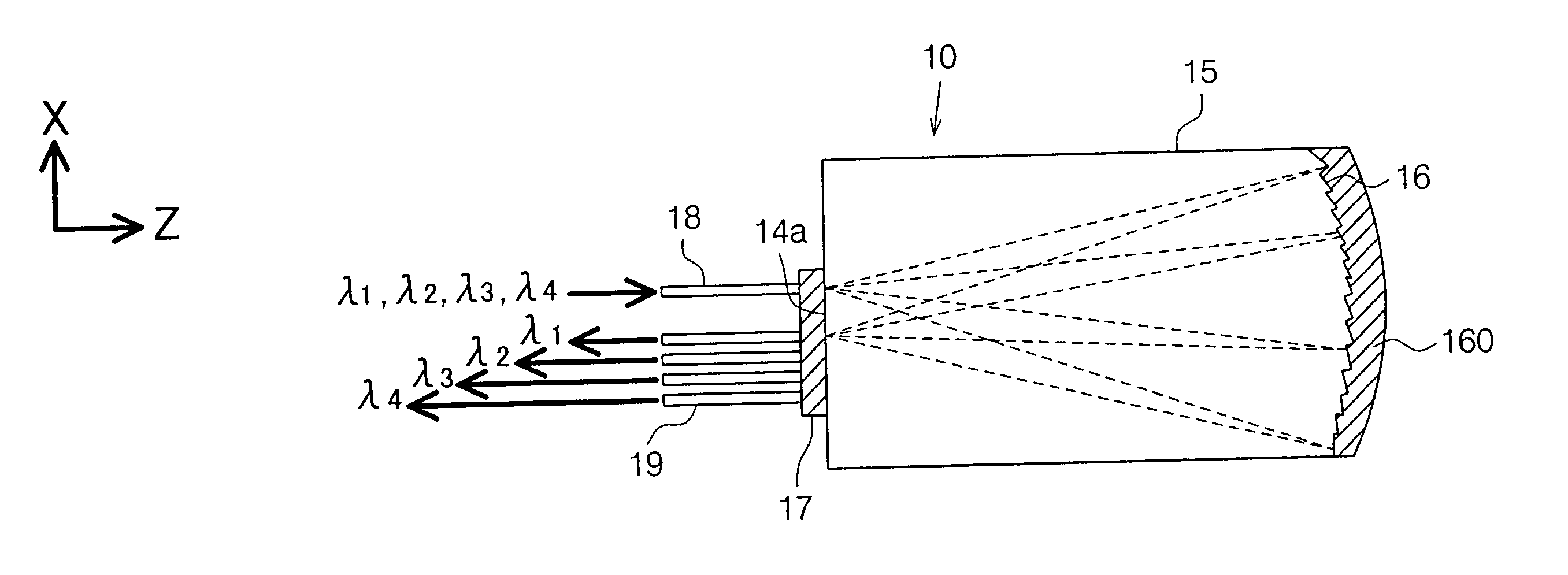
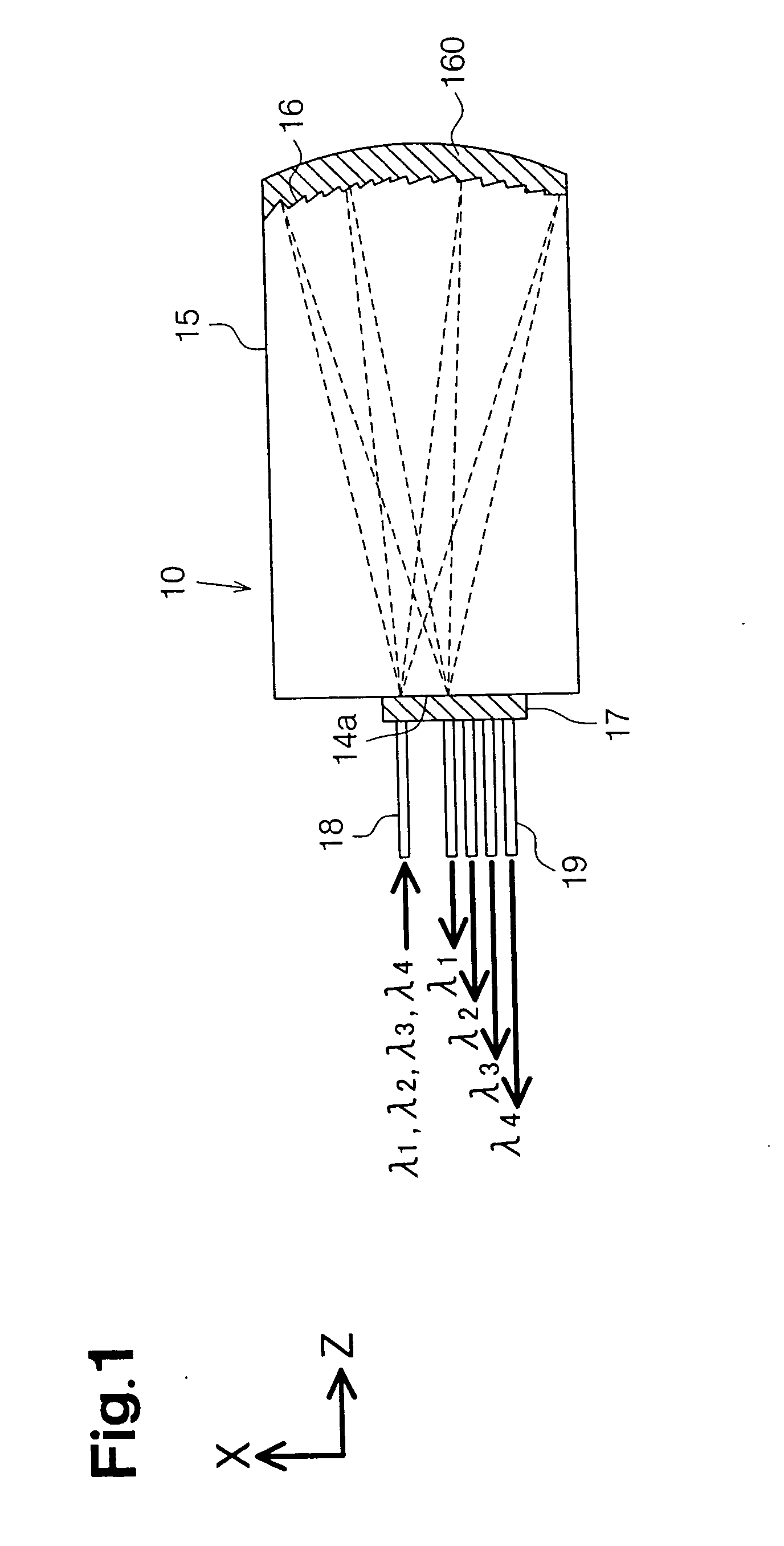
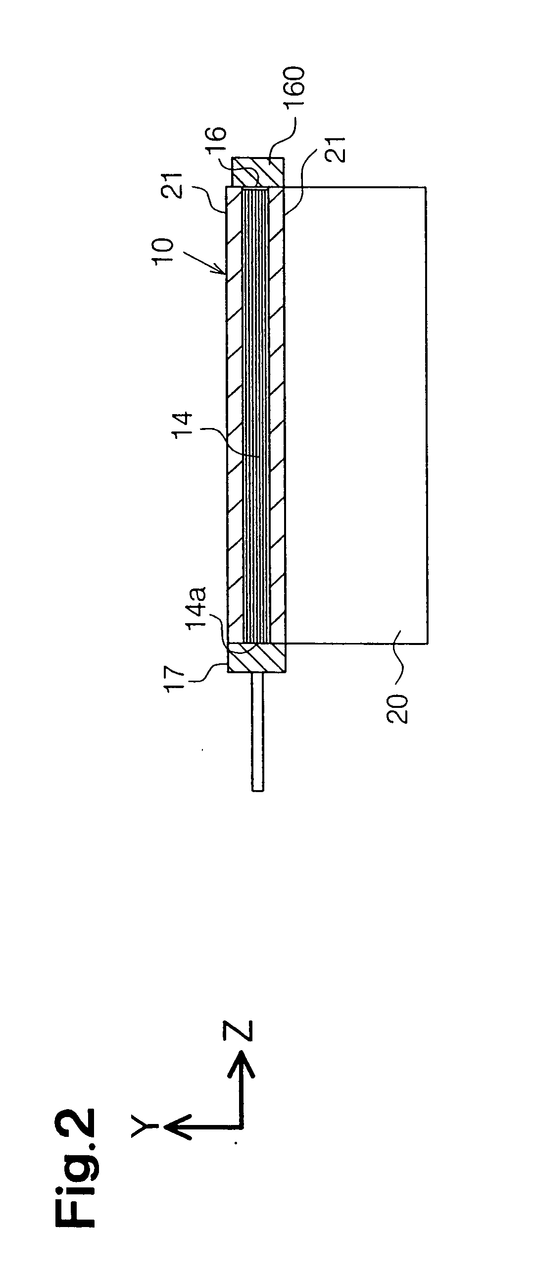
The slab waveguide 15 serves as an input medium contacting the reflective blazed grating 16, which functions as a diffraction grating, and an output medium. The slab waveguide 15 is formed by a one-dimensional photonic crystal having a period characteristic in a single direction (Y axis direction) in which the wavelength of a wave propagated relative to the frequency of the incident wave changes greatly. Thus, an angular difference larger than the normal diffraction device is obtained in the same manner as in the above example (a). Further, the resolution (λ0 / Δλ) corresponding to the frequency of the separated frequencies is drastically decreased. Accordingly, the product of the order m required by the refraction light and the number of steps N may be small. This enables the reflective blazed grating 16 to have a reduced size and improved resolution.

The photonic crystal 14 satisfies the condition in which the absolute value ...

second embodiment

[Second Embodiment]

A diffraction device using a photonic crystal according to a second embodiment of the present invention will now be discussed with reference to FIGS. 3 and 4.

A diffraction device 10A using a photonic crystal shown in FIGS. 3 and 4 is embodied in a multiplexer / demultiplexer having the first feature of the present invention and has a structure corresponding to example (d). In the description of the second embodiment, components that are the same as the corresponding components of the first embodiment are denoted with the same reference numeral and the alphabet “A” following the numeral. Such components will not be described.

In the first embodiment, the light (the light in which optical signals λ1 to λ4 having a plurality of frequencies are multiplexed) transmitted by the input optical fiber 18 enters the slab waveguide 15 from the end of the input optical fiber 18 through the input surface 14a via the phase grating 17. The incident wave is propagated by the hig...

third embodiment

[Third Embodiment]

A diffraction device using a photonic crystal according to a third embodiment of the present invention will now be discussed with reference to FIG. 5 and FIG. 6.

A diffraction device 10 using the photonic crystal of FIGS. 5 and 6 is embodied in a multiplexer / demultiplexer having the first feature of the present invention and has a structure corresponding to example (d). In the description of the third embodiment, components that are the same as the corresponding components of the first embodiment are denoted with the same reference numeral and the alphabet “B” following the numeral. Such components will not be described.

The diffraction device 10B of the third embodiment differs from the second embodiment of FIG. 3 in that the diffraction grating surface of the reflective blazed grating 16B has the concave mirror shape of the first embodiment of FIG. 1 and in that the lens element for incident beam to an input surface of the slab waveguide 15A is only the cylind...


PUM


Abstract

A diffraction device using a photonic crystal includes a diffraction grating, which has a period and periodically divides electromagnetic waves, and an input medium and an output medium, which contact the diffraction grating. The input medium is air, and the output medium is a one-dimensional layer having a periodic characteristic in a single direction (Z axis direction). The photonic crystal is formed by a periodic multilayer film having a period corresponding to the sum of the thickness of a first substance and the thickness of a second substance, which are superimposed. The diffraction device drastically decreases the resolution corresponding to the difference of the separated frequencies.

Description

BACKGROUND OF THE INVENTION The present invention relates to a diffraction device, such as a spectroscope or a diffraction grating, for use in a spectral composition separating device, such as a demultiplexer, that separates an electromagnetic wave in accordance with differences in frequency. When periodically dividing the wave front of an electromagnetic wave for light or the like, it is well known that phase differences produce diffraction waves. Thus, a diffraction grating for periodically dividing the wave front of an electromagnetic wave is widely used in spectroscopes or a diffraction lenses. In recent years, rapid progress has been made in the field of optical communication with technology for dense wavelength division multiplexing (DWDM). In this field, a diffraction grating is widely used since signals having very close wavelengths must be split or coupled. In addition to having a high resolution, the demultiplexer and multiplexer must be compact and inexpensive. When di...

Claims


Application Information

Patent Timeline
IPC IPC(8): G02B5/18G02B6/12G02B6/122G02B6/293G02B6/34
CPCB82Y20/00G02B6/12007G02B6/29328G02B6/1225G02B6/12014
Inventor KITTAKA, SHIGEOOYA, KAZUAKITSUNETOMO, KEIJISERIKOV, VLADIMIR V.
Owner NIPPON SHEET GLASS CO LTD
Features
  • Generate Ideas
  • Intellectual Property
  • Life Sciences
  • Materials
  • Tech Scout
  • Unparalleled Data Quality
  • Higher Quality Content
  • 60% Fewer Hallucinations
Learn More