Electro-luminescence device including a thin film transistor and method of fabricating an electro-luminescence device

Active Publication Date: 2005-01-20
SAMSUNG DISPLAY CO LTD
View PDF2 Cites 17 Cited by
  • Summary
  • Abstract
  • Description
  • Claims
  • Application Information

AI Technical Summary

Benefits of technology

[0023] In at least one embodiment of the invention, the data bus line, the power supply line, the first and second drain electrodes, and the first and second source electrodes are formed simultaneously by etching a source/drain metal thin layer formed over first and second semiconductor layers. The first, second, third, fourth, fifth and sixth semiconduc

Problems solved by technology

However, CRT image displays have disadvantages, such as, for example, flickering, heavy weight, large physical size, and high power consumption.
When a semiconductor layer of a thin film transistor used in a conventional organic electro-luminescence display device is formed using polysilicon, or is formed in the LDD structure, the thin film transistor may have a complicated structure, the manufacturing time for the thin film transistor m

Method used


Image

  • Electro-luminescence device including a thin film transistor and method of fabricating an electro-luminescence device
  • Electro-luminescence device including a thin film transistor and method of fabricating an electro-luminescence device
  • Electro-luminescence device including a thin film transistor and method of fabricating an electro-luminescence device

Examples


Embodiment Construction

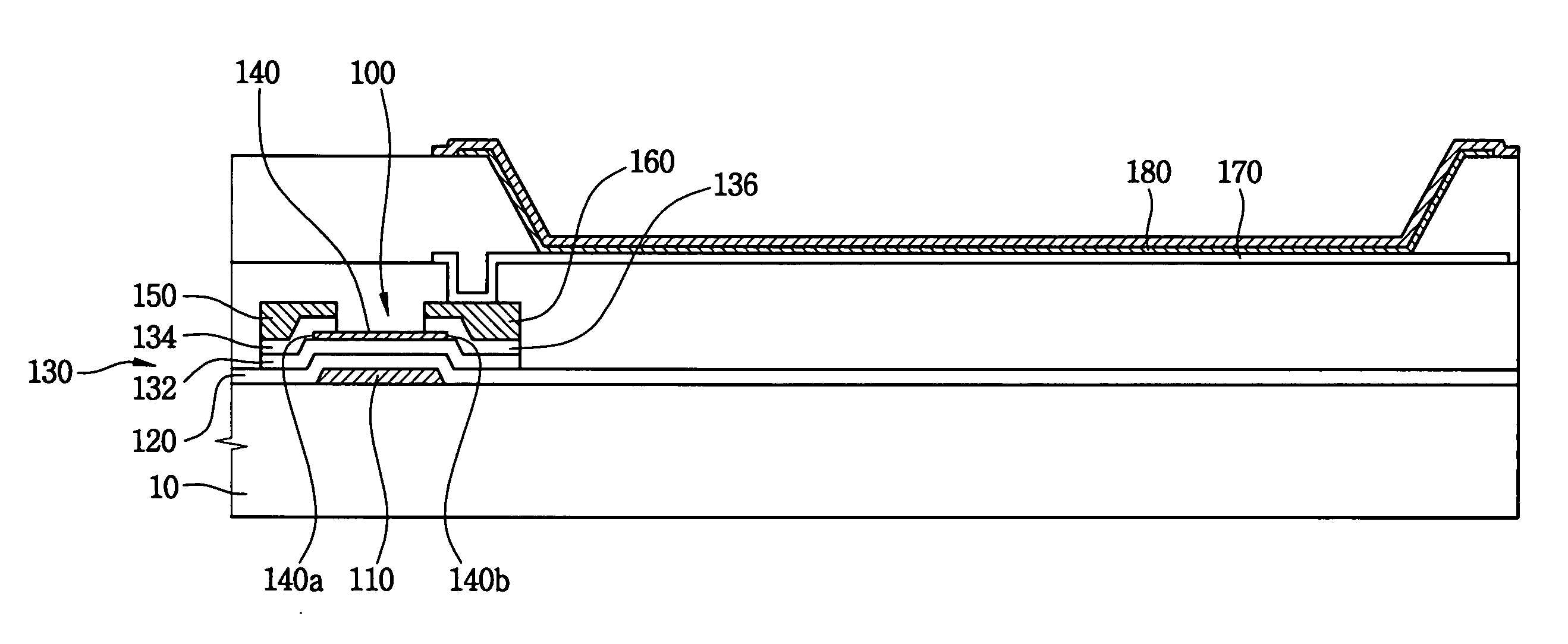
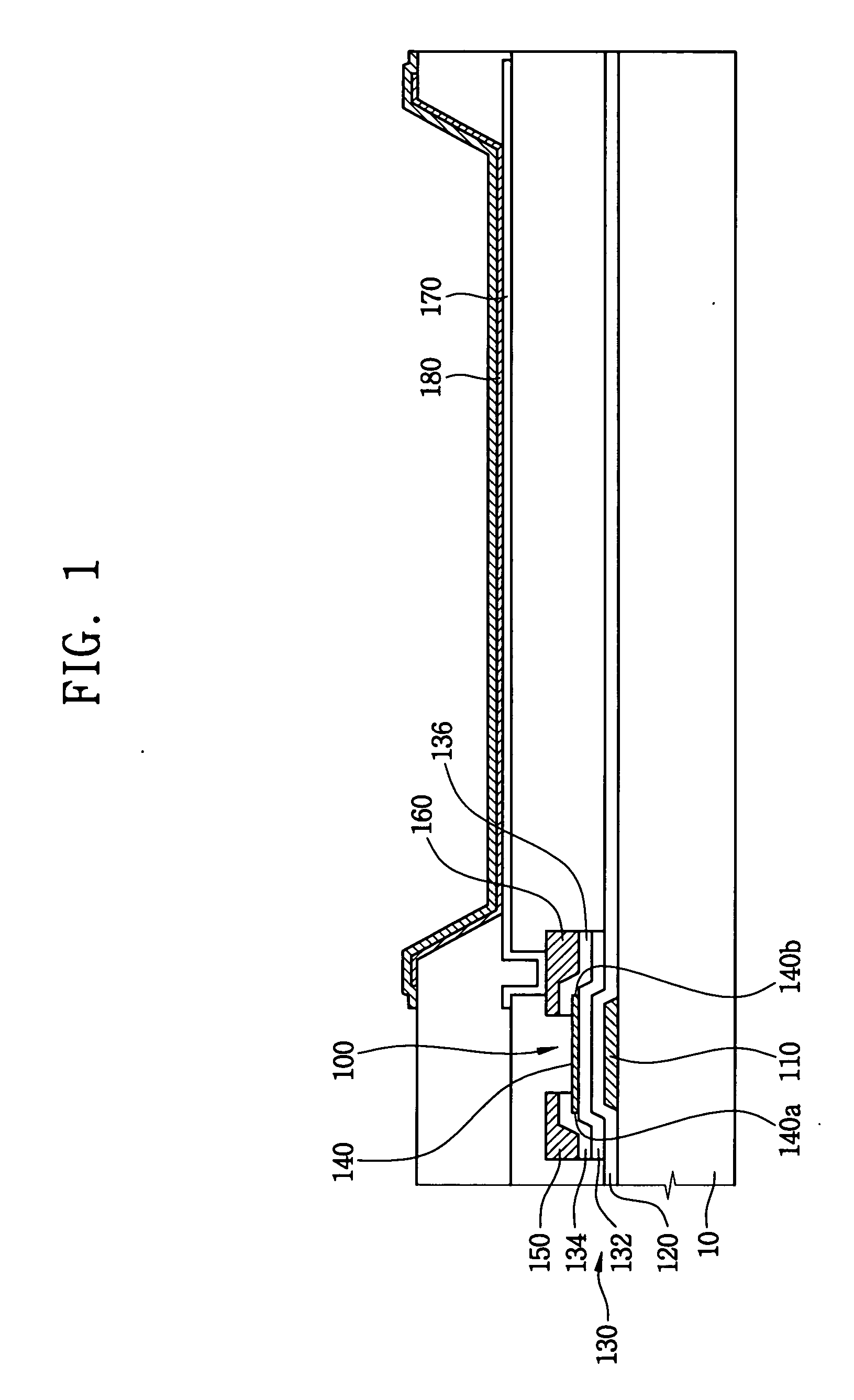
[0039]FIG. 1 is a schematic cross-sectional view of a thin film transistor for an electro-luminescence device according to an exemplary embodiment of the present invention.

[0040] Referring to FIG. 1, a thin film transistor 100 according to the present embodiment of the invention includes a first electrode 110, an insulating layer 120, a semiconductor pattern 130, an etch stop layer 140, a second electrode 150 and a third electrode 160. The thin film transistor 100 is formed on a substrate 10.

[0041] The first electrode 110 is formed on the substrate 110 using a conductive thin film layer having low electric resistance, such as, for example, aluminum, aluminum alloy, copper, or copper alloy. The first electrode 110 receives a voltage higher than a threshold voltage of the semiconductor pattern 130 to lower the electric resistance of the semiconductor pattern 130.

[0042] The insulating layer 120 is formed over the substrate 10 to cover the first electrode 110. The insulating layer 12...


PUM


Abstract

An electro-luminescence device including an electro-luminescence element and a thin film transistor electrically connected to the electro-luminescence element. The thin film transistor includes a gate electrode formed over a substrate, an insulating layer formed over the gate electrode, and a first semiconductor pattern formed over the insulating layer. An etch stop layer is formed over the first semiconductor layer. A second semiconductor pattern is formed over the etch stop layer at one side of the etch stop layer, and a third semiconductor pattern is formed over the etch stop layer at another side of the etch stop layer. A source electrode is formed over the second semiconductor pattern, and a drain electrode is formed over the third semiconductor pattern.

Description

CROSS-REFERENCE TO RELATED APPLICATION [0001] This application claims priority based upon Korean Patent Application No. 2003-49400 filed on Jul. 18, 2003. BACKGROUND [0002] 1. Technical Field [0003] The present disclosure relates to a thin film transistor (TFT) for an electro-luminescence (EL) device and a method of fabricating the same. [0004] 2. Disclosure of Related Art [0005] Display devices have many applications and act as an interface between electrical devices, such as computers and televisions, and a user. Display devices operate by changing information in the form of electrical signals into an image and providing the image to the user. [0006] Display devices may be classified into an emissive display device, such as, for example, a cathode ray tube (CRT), a plasma display panel (PDP), a light emitting diode (LED), and an organic electro-luminescent display device (ELD), or a non-emissive display device, such as, for example, a liquid crystal display (LCD), an electrochemic...

Claims


Application Information

Patent Timeline
IPC IPC(8): H01L21/311H01L51/50H01L21/336H01L27/32H01L29/786H05B33/00H05B33/10H05B33/12H05B33/14
CPCH01L27/3262H01L27/3244H10K59/1213H10K59/12H05B33/00
Inventor CHOI, JOON-HOOJOO, IN-SUCHOI, BEOM-RAKHUH, JONG-MOO
Owner SAMSUNG DISPLAY CO LTD
Why Eureka
Try Eureka