Semiconductor integrated circuit

a technology of integrated circuits and semiconductors, applied in the direction of logic circuit coupling/interface arrangements, semiconductor devices, semiconductor/solid-state device details, etc., can solve the problems of reducing the switching speed of transistors, unable to achieve the speeding up of output circuits in second prior art, and unable to achieve output circuit speeding up, etc., to achieve the effect of sacrificing esd performance, high resistance region, and eliminating output transistors

Inactive Publication Date: 2005-01-27
NEC ELECTRONICS CORP
View PDF8 Cites 21 Cited by
  • Summary
  • Abstract
  • Description
  • Claims
  • Application Information

AI Technical Summary

Benefits of technology

[0013] The above-mentioned first prior art has a problem that speeding up of the output circuit can not be achieved since the parasitic capacitance of the drain portion increases due to the N-well provided in the drain of the output transistor, so that the switching speed of the transistor is lowered. A countermeasure which is similar to that of the first prior art is also required since an ESD current flows due to the operation of the parasitic bipolar transistor in a protection element if a silicide film is formed on the diffused layer. The second prior art also can not achieve the speeding up of the output circuit. Damaging of the gate oxide film due to ESD stress between the output pin and the power supply terminal is expected since the gate electrode of the NMOS transistor which is constantly conductive is connected to the power supply terminal VDD. In the CMOS high technology of 90 nm node generation in which the thickness of the gate oxide film is about 1.6 nm, provision of a protection circuit also between the output pin and the power supply terminal is essential. Thus, formation of a parasitic capacitance due to the presence of a protection circuit between the output pin and the power supply terminal prevents speeding up of the output circuit.
[0017] Since the high resistance region between the output pin and the output transistor can be eliminated without sacrificing the ESD performance in accordance with the present invention, it is possible to reduce the size of the diffused layer of the MOS transistor which is connected to the output pin to the manufacturing limit for siliciding the entire area of the diffused layer. Since the gate electrodes of the output circuit is not connected to the power supply terminal and ground terminal, but all the gate electrodes are connected to the internal circuit, the ESD current to the output current is easy to uniformly flow. Accordingly, ESD damage of the output circuit per se can be prevented and the ESD protection circuit between the output pin and the power supply terminal can be eliminated. Therefore, the capacitance and resistance of the parasitic diffused layer in the output circuit can be made very low, so that high speed operation of the output circuit can be made possible. In the prior art, if the Human-Body-Model electrostatic discharge withstand voltage (HBM-ESD withstand voltage) is 200 V in the output pin of the 90 nm node CMOS semiconductor integrated circuit, a parasitic capacitance of about 4 PF occurs. High speed operation is not possible unless the electrostatic discharge withstand voltage is sacrificed. However, in the output terminal to which the present invention is applied, high speed signal operation of about 10 Gbps is possible while suppressing the parasitic capacitance to 0.1 PF or less and meeting the requirement of HBM-ESD withstand voltage of 2000 V or more.

Problems solved by technology

The above-mentioned first prior art has a problem that speeding up of the output circuit can not be achieved since the parasitic capacitance of the drain portion increases due to the N-well provided in the drain of the output transistor, so that the switching speed of the transistor is lowered.
The second prior art also can not achieve the speeding up of the output circuit.

Method used


Image

  • Semiconductor integrated circuit
  • Semiconductor integrated circuit
  • Semiconductor integrated circuit

Examples


Embodiment Construction

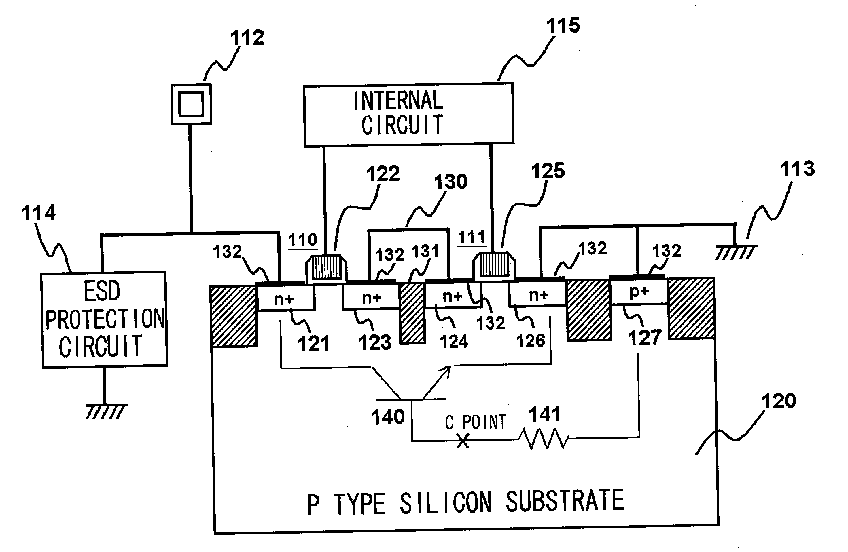
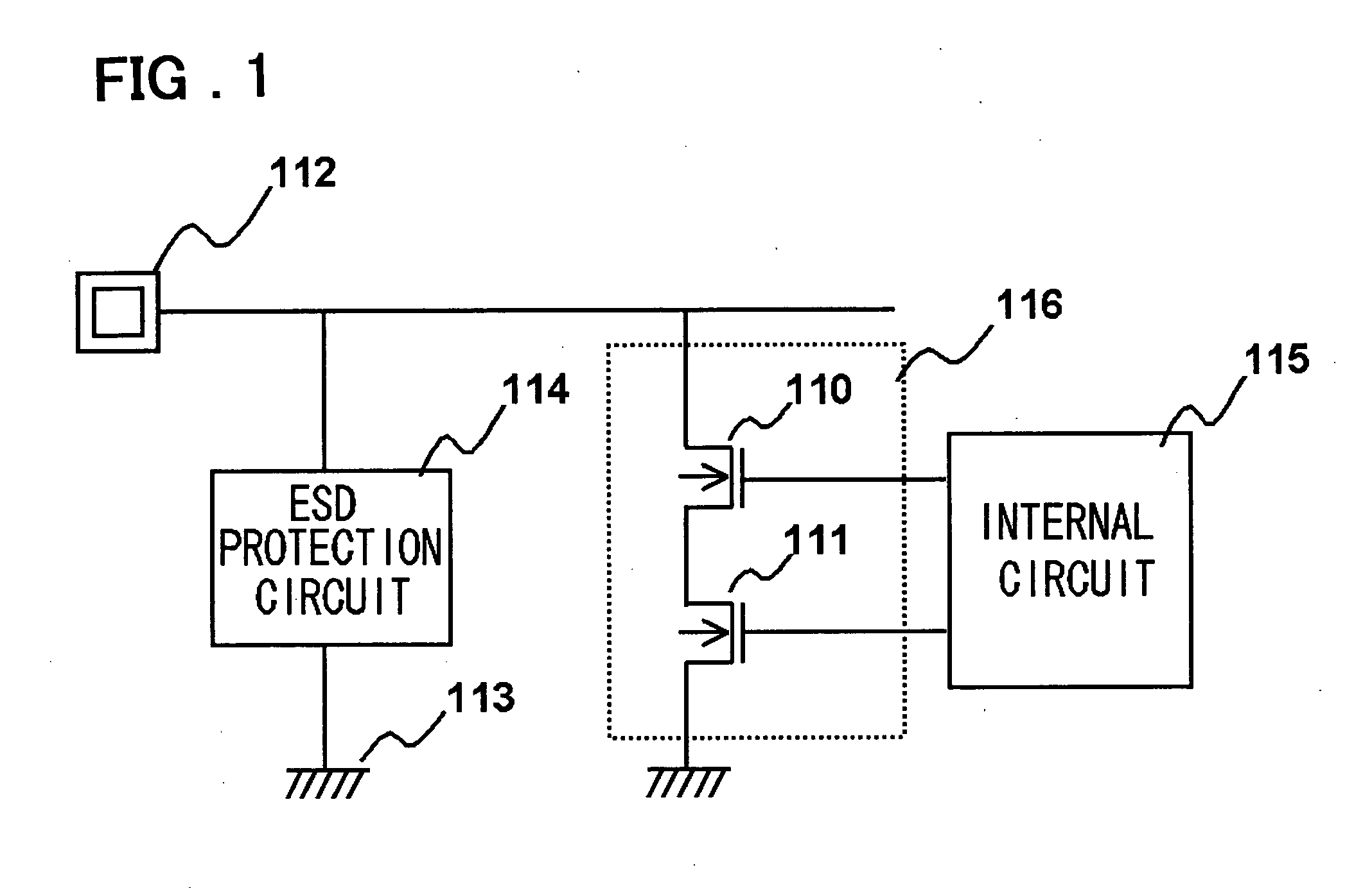
[0029] A first embodiment of the present invention will now be described with reference to the drawings. FIG. 1 is a circuit diagram showing main components of a first embodiment. A reference numeral 112 in FIG. 1 denotes an output terminal of a semiconductor integrated circuit. A numeral 114 denotes a devoted ESD protection circuit between the output pin 112 and the ground terminal 113; 115 denotes an internal circuit; 110 denotes a first NMOS transistor; 111 denotes a second NMOS transistor. The first NMOS transistor 110 is cascade connected to the second NMOS transistor 111, so that they constitute an output circuit 116 for outputting a signal from the internal circuit 115. Both first and second NMOS transistors 110 and 111 have their gate electrodes which are connected to the internal circuit 115.

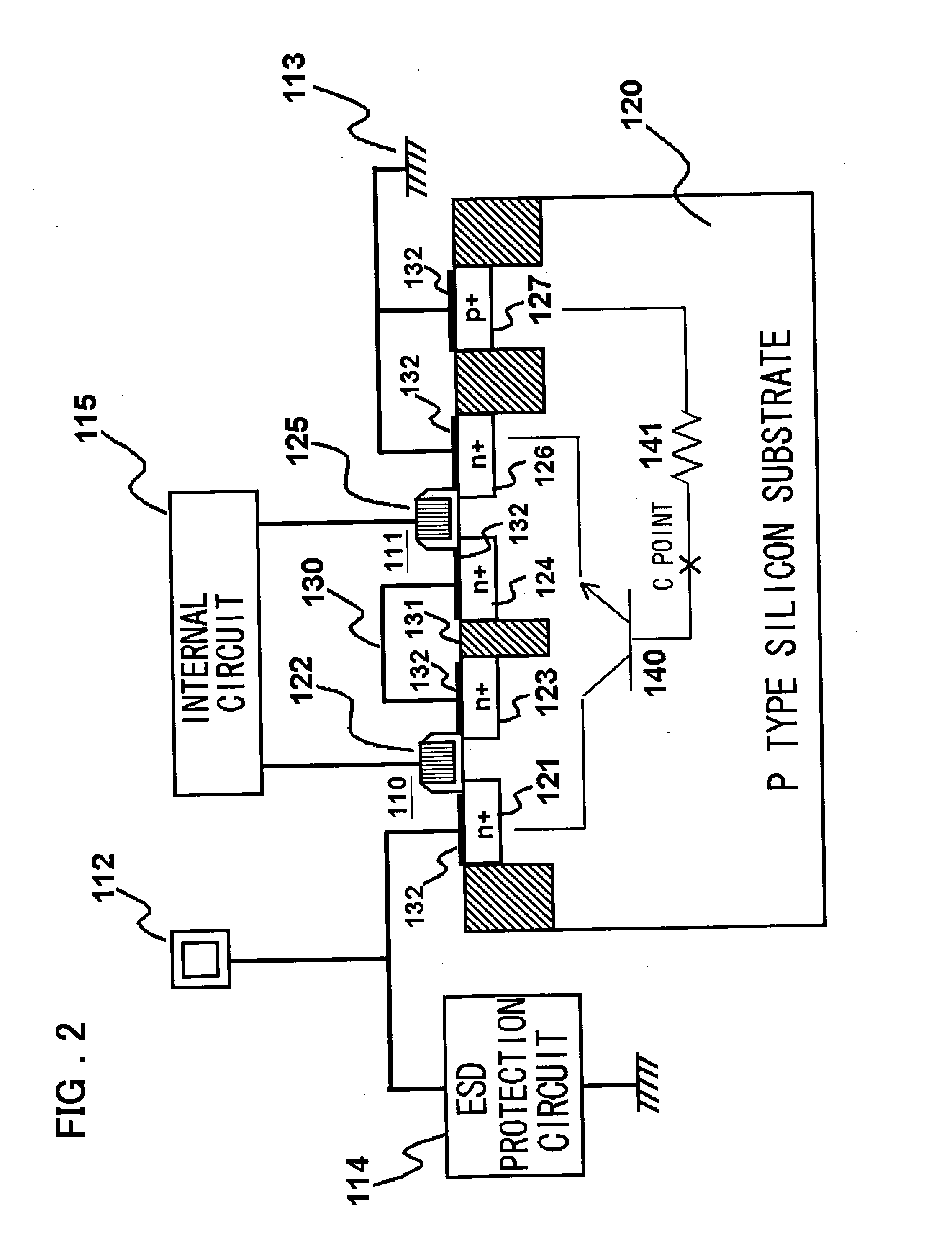
[0030]FIG. 2 is a sectional view showing main components of the first embodiment. The first and second NMOS transistors NMOS transistors 110 and 111 are formed on the P type substrate ...


PUM


Abstract

To provide an output circuit having a low parasitic capacitance and resistance in the drains of output transistors, which is operable at a high speed and its ESD performance is improved. A devoted electrostatic discharge protection circuit is provided between the output terminal (pin) and the ground terminal (or power supply terminal). An output circuit which is in parallel connected to this electrostatic discharge protection circuit comprises a first and second MOS transistors which are cascade-connected to each other. The entire area of the source / drain regions of the first and second MOS transistors are silicided. Both transistors have their gate electrodes which are connected to an internal circuit. The source doped region of the first MOS transistor is separated from the drain doped region of the second MOS transistor and they are connected to each other by metal wiring.

Description

FIELD OF THE INVENTION [0001] The present invention relates to a semiconductor integrated circuit and in particular to a semiconductor integrated circuit having high speed output circuitry, the electrostatic discharge performance of which is improved. BACKGROUND OF THE INVENTION [0002] Recently, the sizes of MOS transistors which form semiconductor integrated circuits have been made smaller. The fact that the reduced thickness of the gate insulating films and the shallow PN junctions of the transistors, which is associated with the reduction in the size thereof makes it more difficult to prevent the semiconductor integrated circuit from damaging due to electrostatic discharge (ESD). An improvement in performance of the ESD protection circuit is essential to prevent breakdown due to electrostatic discharge. [0003] In order to make the resistance of the source-drain diffused layer lower in a association with reduction in size, a technique to provide a silicide layer on the diffused la...

Claims


Application Information

Patent Timeline
Patent Type & Authority Applications(United States)
IPC IPC(8): H01L27/04H01L21/822H01L21/8234H01L23/60H01L23/62H01L27/02H01L27/06H01L27/07H01L27/088H03K19/0175
CPCH01L23/60H01L27/0266H01L27/0716H01L27/088H01L2924/0002H01L2924/3011H01L2924/00H03K19/0175
Inventor MORISHITA, YASUYUKI
Owner NEC ELECTRONICS CORP
Why Eureka
Try Eureka