Optical multilayer-film filter, method for fabricating optical multilayer-film filter, optical low-pass filter, and electronic apparatus

Inactive Publication Date: 2005-01-27
SEIKO EPSON CORP
View PDF0 Cites 44 Cited by
  • Summary
  • Abstract
  • Description
  • Claims
  • Application Information

AI Technical Summary

Benefits of technology

One object of the present invention, among others, is to provide an optical multilayer-film filter that has better prevention of the optical strain due to stresses of the dielectric thin films laminated on the transparent substrate, and has reduced warp width of the substrate. Another object is to provide a method for fabricating such an advantageous optical multilayer-film filter.
With the above-described structure, because of being composed of a silicon-oxide—base compound, the dielectric monolayer film provides a monolayer film shaving a strong compressive stress, thereby achieving an optical multilayer-film filter having reduced warp width.
According to the method for fabricating an optical multilayer-film filter, an optical multilayer-film filter having a warp width less than-that of the known optical multilayer-film filter is easily fabricated.

Problems solved by technology

However, the light in the infrared region is invisible to the human eye and unnecessary for the normal use of a camera.
Furthermore, near-infrared light incident on an image-capturing device causes problems such as a reduction in resolution and an unevenness in an image.
An infrared-cut filter composed of color glass, however, is an independent component, and its own respective size tends to limit the overall reduction in size that can be achieved in the optical system.
However, such an optical multilayer-film filter is problematic to manufacture because the two dielectric multilayer films have large and mutually different numbers of layers.
Also, this kind of proposed filter has a problem from the viewpoint of a tradeoff with the optical characteristics.
That is to say, this kind of filter is unlikely to achieve a well-balanced relation between the stresses of the dielectric multilayer films laminated on both surfaces of the transparent substrate, thereby leading to an unsatisfactory reduction in the warp width of the transparent substrate.

Method used


Image

  • Optical multilayer-film filter, method for fabricating optical multilayer-film filter, optical low-pass filter, and electronic apparatus
  • Optical multilayer-film filter, method for fabricating optical multilayer-film filter, optical low-pass filter, and electronic apparatus
  • Optical multilayer-film filter, method for fabricating optical multilayer-film filter, optical low-pass filter, and electronic apparatus

Examples


first embodiment

A first exemplary embodiment of the invention is taught in relation to the application of the concepts of the invention in an optical multilayer-film filter (UV-IR cut filter) which allows light in the visible wavelength region to be transmitted therethrough, and which has an excellent reflecting characteristic of absorbing very little light having wavelengths between the UV and IR wavelength regions. That is to say, very little light not longer than a predetermined wavelength, in the ultraviolet wavelength region, and light having wavelengths not shorter than a predetermined wavelength, in the infrared wavelength region, is absorbed.

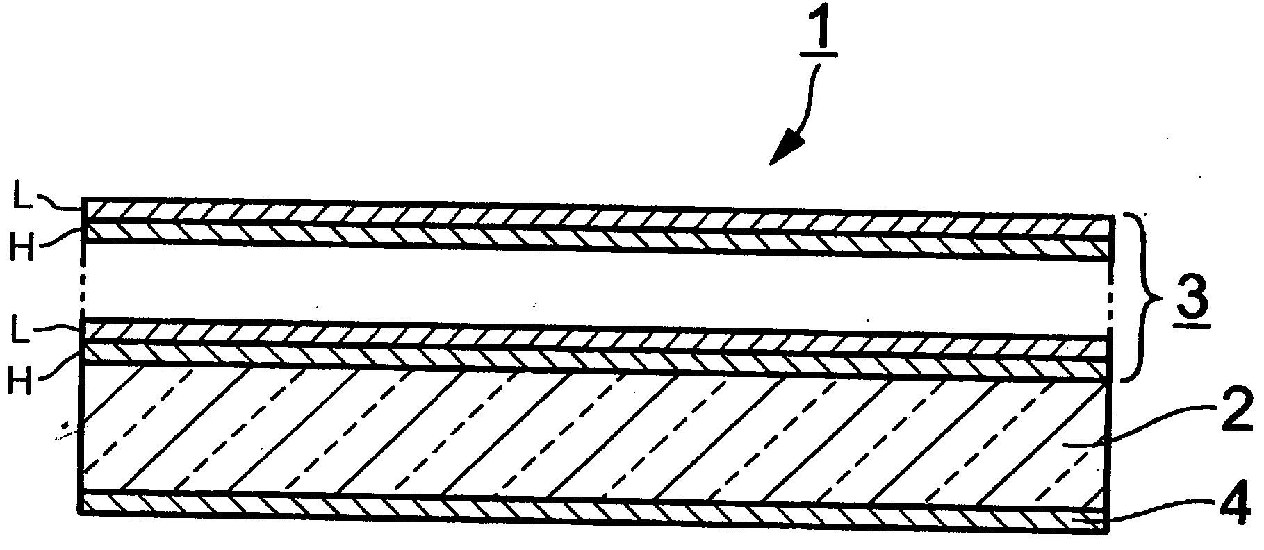
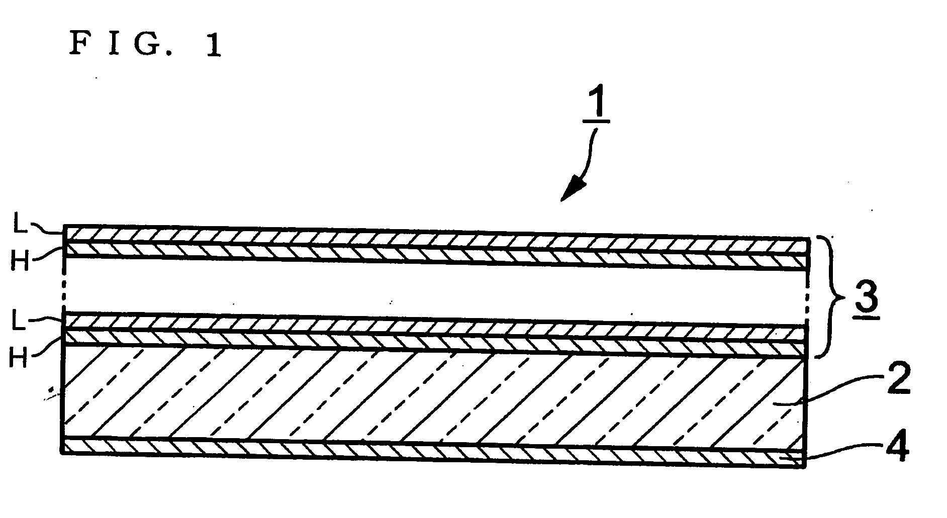
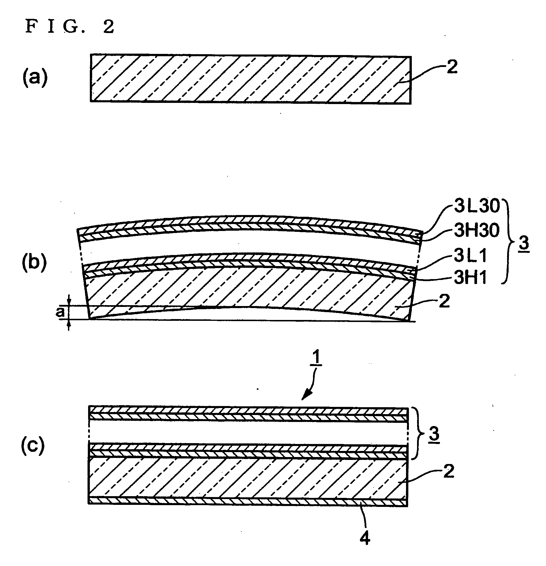
The discussion will now involve FIG. 1, which is a schematic sectional view of the structure of an optical multilayer-film filter according to an embodiment of the present invention, and FIG. 2, which illustrates a method for fabricating the optical multilayer film filter.

As shown in FIG. 1, an optical multilayer-film filter 1 has a substrate 2 all...

second embodiment

The second embodiment is different, from the first embodiment only in that the substrate is composed of quartz crystal.

The substrate allowing light to be transmitted therethrough is composed of a piece of quartz crystal (transmittance: n=1.52) having a two-dimensional size of 48 mm×43 mm and a thickness of 0.43 mm. The second embodiment is one embodiment applied to a UV-IR cut filter while being arranged such that the conditions thereof other than the material of the substrate are generally the same as those in the first embodiment.

The quartz crystal substrate having the dielectric multilayer film 3 formed thereon tends to be upwardly warped due to the strong compressive stresses of the low-refractive-index material layers (composed, e.g., of SiO2) and the weak tensile stresses of the high-refractive-index material layers (composed, e.g., of TiO2). The dielectric multilayer film 3 thus tends to have a surface with an upwardly protruding shape.

Next, with the dielectric multilaye...

third embodiment

The third embodiment is one embodiment applied to an optical multilayer-film filter (IR cut filter) which allows light in the visible wavelength region to be transmitted therethrough and has an excellent reflecting characteristic of absorbing little light in the infrared wavelength region, having wavelengths not shorter than a predetermined wavelength.

The third embodiment is different from the first embodiment only in the number of film layers and the film thickness structure of the dielectric multilayer film 3 formed on the upper surface of the glass substrate 2 and the film thickness structure of the dielectric monolayer film 4 formed on the lower surface of the glass substrate 2.

A method for forming films on the glass substrate in the third embodiment will be described below. With respect to the formation of the dielectric multilayer film 3 on the glass substrate 2, each high-refractive-index material layer (H) is composed of TiO2 and each low-refractive-index material layer (...


PUM


Abstract

An optical multilayer-film filter formed by laminating dielectric thin films on a transparent substrate has a structure in which a dielectric multilayer film formed by alternately laminating high-refractive-index material layers and low-refractive—index material layers is formed on one surface of the transparent substrate, a dielectric monolayer film is formed on the other surface of the transparent substrate, and the dielectric monolayer film is composed of a dielectric material having substantially the same refractive index as that of the transparent substrate. With this structure, a warp width of the substrate due to stresses of the dielectric thin films laminated in the transparent substrate can be further reduced, thereby achieving an optical multilayer-film filter which is protected from optical strain.

Description

TECHNICAL FIELD The present invention relates to an optical multilayer-film filter formed by laminating dielectric thin films, a method for fabricating the optical multilayer-film filter, an optical low-pass filter, and an electronic apparatus. BACKGROUND ART In recent years, image-capturing devices for video cameras, digital cameras, and the like have employed a charge coupled device (CCD). A CCD is sensitive to light in a relatively wide wavelength region. That is, a CCD is sensitive not only to light in a visible region but also in a near-infrared region (750-2500 nm). However, the light in the infrared region is invisible to the human eye and unnecessary for the normal use of a camera. Furthermore, near-infrared light incident on an image-capturing device causes problems such as a reduction in resolution and an unevenness in an image. To cut out the near-infrared part of the incident light, an infrared-cut filter such as a sheet of color glass may be inserted in optical syste...

Claims


Application Information

Patent Timeline
IPC IPC(8): G02B5/28G02B5/30G03B11/00H04N5/225
CPCG02B5/281H04N5/2254G02B5/283
Inventor YANO, KUNIHIKOKAZAMA, MINORUKITAMURA, KEIKO
Owner SEIKO EPSON CORP
Why Eureka
Try Eureka