Method and apparatus for performing failure analysis with fluorescence inks

a technology of fluorescence ink and failure analysis, applied in the field of semiconductor devices, can solve the problems of insufficient contrast of current cross sectioning techniques, inability to determine a point of failure in wafer level chip scale packages (wl-csp's), and in product assembled to organic media, etc., to achieve convenient viewing of cross section faces and easy identification

Inactive Publication Date: 2005-01-27
NXP USA INC
View PDF4 Cites 14 Cited by
  • Summary
  • Abstract
  • Description
  • Claims
  • Application Information

AI Technical Summary

Benefits of technology

[0010] According to one embodiment, a method for performing failure analysis on a semiconductor device under inspection includes preparing of a device sample using an encapsulation material containing a dye, the prepared device sample possibly including a failure area having wicked in encapsulation material containing the dye. The prepared device sample is then sectioned to facilitate viewing a cross section face of the device under inspection. Lastly, a dark field analysis on the prepared device sample is performed with the use of dark field illumination. Responsive to at least one failure area containing wicked in encapsulation material with dye occurring on the cross section face of the device under inspection, the failure area can be readily identified as well as a contrast and perspective of remaining portions of the cross section face being maintained.

Problems solved by technology

Determining a point of failure in wafer level chip scale packages (WL-CSP's), or in product assembled to organic media, can be difficult.
The point of failure may be due to either cracks in solder bumps, delamination of various organic films such as polyimide, bi-cycle butane (BCB), stress compensation layers (SCL) or soldermasks.
Current cross sectioning techniques do no allow sufficient contrast to determine such a point of failure.
In the preceding case, the technique lacks sufficient contrast to determine a point of failure in a wafer level chip scale package.
Fluorescent microscope technology requires costly specialized filter sets, for example, on the order of greater than $1,500.00 per set.
Fluorescent microscope technology also requires high intensity light sources, for example, on the order of greater than 250 W. Furthermore, fluorescent microscope technology used in failure analysis suffers from loss of contrast between a failed area and a remaining section of the device under inspection.
However, contrast of the part under bright light is diminished, tending to render detail of the device under examination and the failure analysis less than optimal.
However, contrast of the part under bright light is diminished, likewise rendering detail of the device under examination and the failure analysis less than optimal.

Method used


Image

  • Method and apparatus for performing failure analysis with fluorescence inks
  • Method and apparatus for performing failure analysis with fluorescence inks
  • Method and apparatus for performing failure analysis with fluorescence inks

Examples


Embodiment Construction

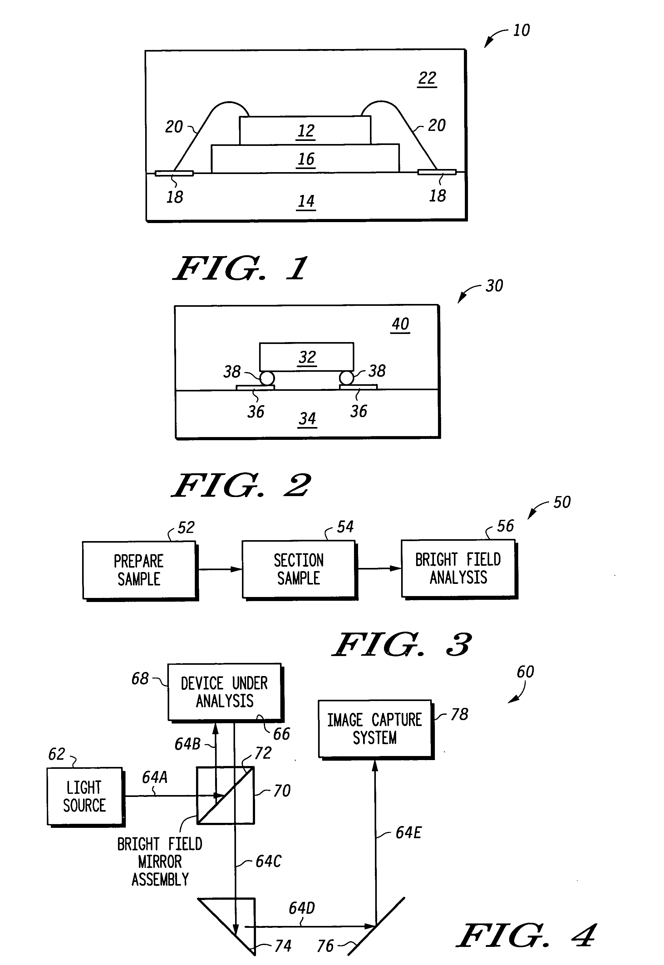
[0021]FIG. 1 is a schematic cross-sectional view of a typical wire bonded and assembled semiconductor device 10. Semiconductor device 10 includes a die 12 physically coupled to substrate 14 via a conventional die attach method such as die attach epoxy 16. In addition, device 10 includes die bond pads 18 disposed on substrate 14, wherein die wire bonds 20 interconnect between die 12 and substrate 14 at respective die bond pads. Furthermore, for performing a failure analysis on device 10, there is provided a mold compound 22 for encapsulating at least die 12, as well as other portions of device 10, as needed.

[0022]FIG. 2 is a schematic cross-sectional view of a flip chip assembled semiconductor device 30. Semiconductor device 30 includes a die 32 physically coupled to substrate 34 via a die attach pads 36 and solder spheres 38. That is, device 30 includes die attach bond pads 36 disposed on substrate 34, wherein the solder spheres 38 interconnect between die 32 and substrate 34 at re...


PUM

PropertyMeasurementUnit
diameteraaaaaaaaaa
temperaturesaaaaaaaaaa
sizeaaaaaaaaaa

Abstract

A method for performing failure analysis on a semiconductor device under inspection includes preparing of a device sample using an encapsulation material containing a dye, the prepared device sample possibly including a failure area having wicked in encapsulation material containing the dye. The prepared device sample is then sectioned to facilitate viewing a cross section face of the device under inspection. Lastly, a dark field analysis on the prepared device sample is performed with the use of dark field illumination. Responsive to at least one failure area containing wicked in encapsulation material with dye occurring on the cross section face of the device under inspection, the failure area can be readily identified as well as a contrast and perspective of remaining portions of the cross section face being maintained.

Description

BACKGROUND [0001] 1. Field of the Invention [0002] The present disclosure relates to semiconductor devices, and more particularly, to a method and apparatus for performing failure analysis of semiconductor devices with fluorescence inks. [0003] 2. The Related Art [0004] Determining a point of failure in wafer level chip scale packages (WL-CSP's), or in product assembled to organic media, can be difficult. The point of failure may be due to either cracks in solder bumps, delamination of various organic films such as polyimide, bi-cycle butane (BCB), stress compensation layers (SCL) or soldermasks. Current cross sectioning techniques do no allow sufficient contrast to determine such a point of failure. [0005] As known in the art, fluorescence microscopy is performed at narrow emission and excitation wavelengths, usually confined to medical and biological applications. Other reported work is in the field of metallography in the determination of metal porosity. In the preceding case, th...

Claims


Application Information

Patent Timeline
Patent Type & Authority Applications(United States)
IPC IPC(8): G01N21/91G06K9/00
CPCG01N21/91
Inventor WHITE, JERRY L.LEE, RUSSELL T.
Owner NXP USA INC
Why Eureka
Try Eureka