Method of selecting photomask blank substrates

a technology of photomask and substrate, which is applied in the field of selecting substrates for photomask blanks, can solve the problems of reducing the accuracy of photolithographic processes employed in semiconductor manufacturing, the flatness of the photomask used in lithography, and the inability to ignore the flatness of the substrate as a cause of focal shift, so as to reduce the minimum feature size and high accuracy

Active Publication Date: 2005-01-27
SHIN ETSU CHEM IND CO LTD +2
View PDF3 Cites 21 Cited by
  • Summary
  • Abstract
  • Description
  • Claims
  • Application Information

AI Technical Summary

Benefits of technology

[0010] It is therefore one object of the invention to provide a method of selecting photomask blank substrates capable of giving photomasks which can be used to expose patterns having a reduced minimum feature size to a high accuracy on a wafer substrate.

Problems solved by technology

These trends have led to a number of technical challenges concerning the accuracy of photolithographic processes employed in semiconductor manufacturing.
One such challenge relates to the flatness of the photomask used in lithography.
As the minimum feature size becomes smaller, the focal depth allowed by the resist becomes smaller, making it impossible to disregard the flatness of the substrate as a cause of focal shift.
Nor has anything been known about what sort of method may be used to form such a surface shape so as to enable the production of substrates having the desired surface shape in a good yield or about how to suppress the formation of defects on the substrate itself or of photomask defects that originate from the substrate.

Method used


Image

  • Method of selecting photomask blank substrates
  • Method of selecting photomask blank substrates
  • Method of selecting photomask blank substrates

Examples


example 1

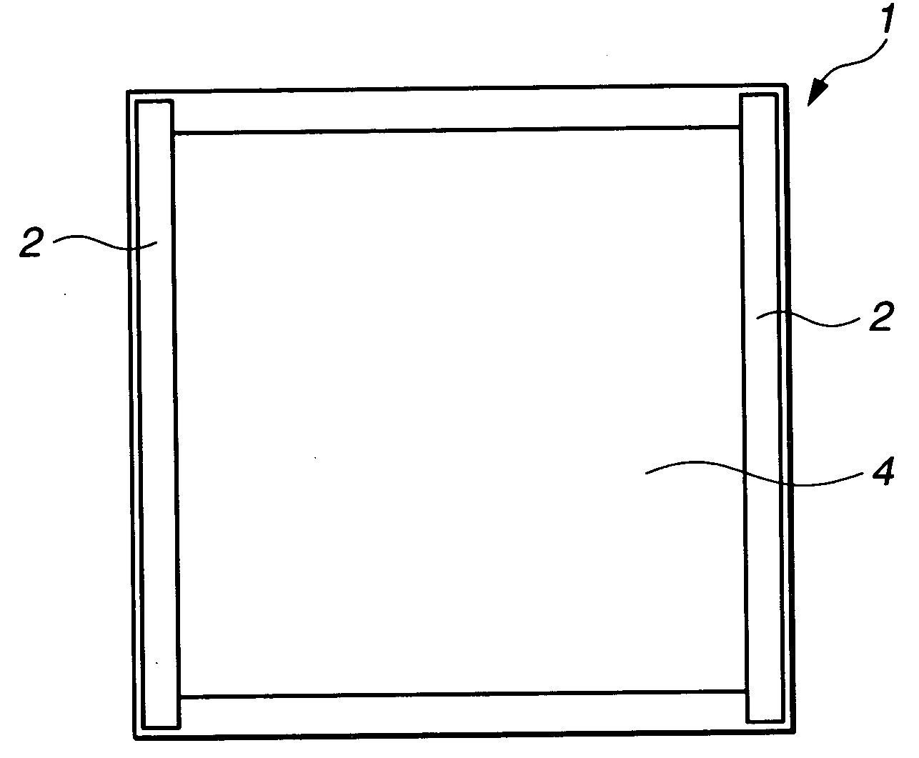
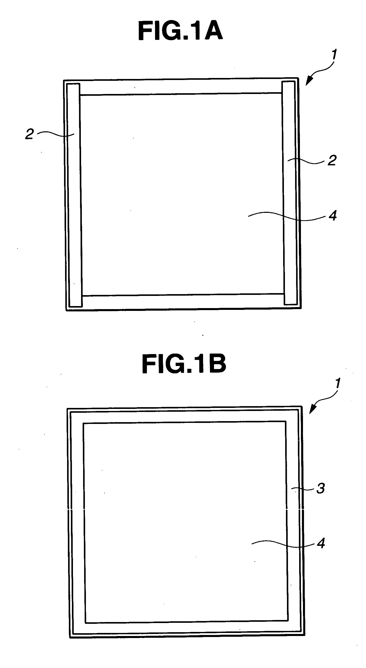
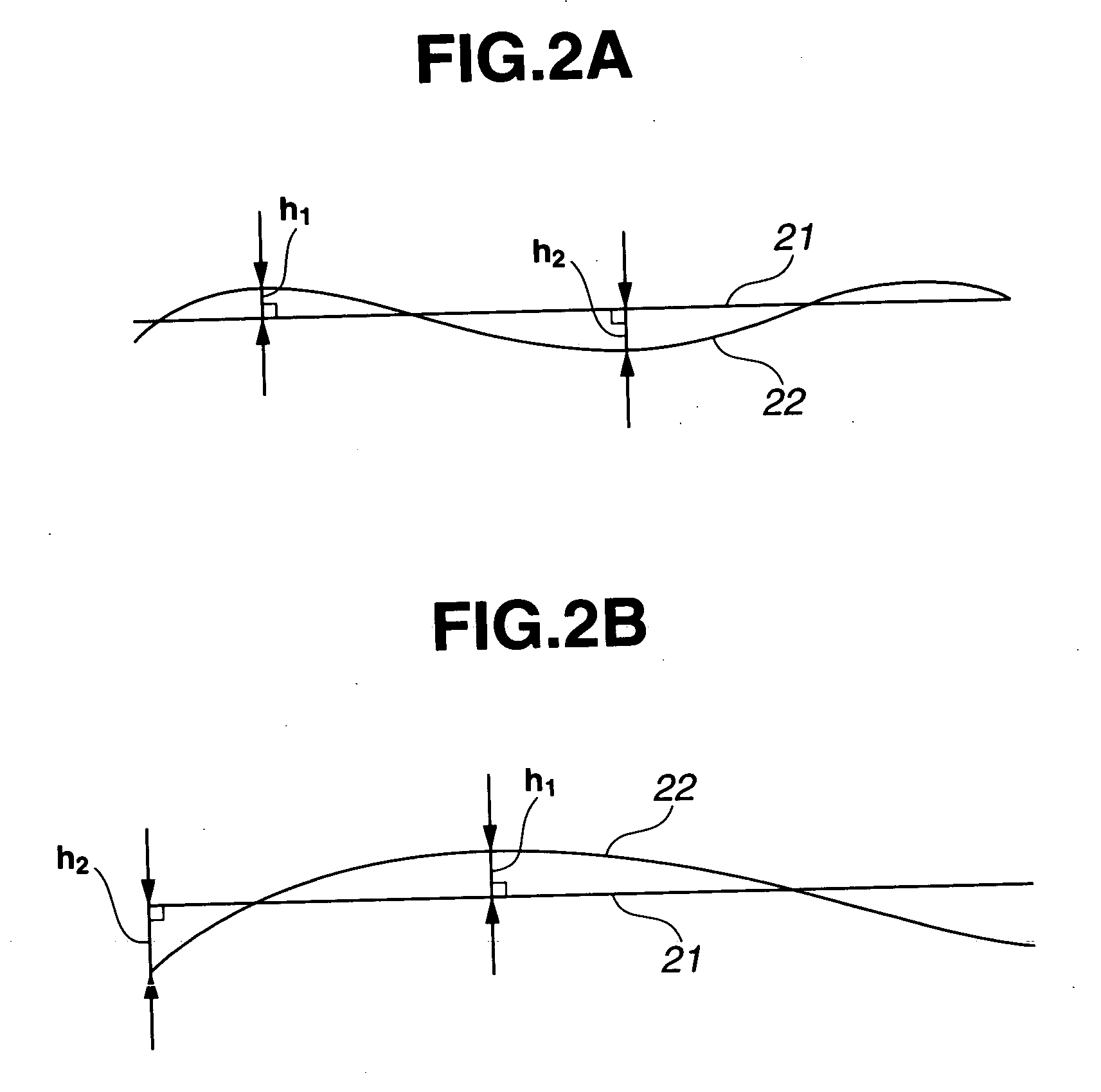
[0078] Using a flatness tester, the height of a principal surface region on 152 mm (6 inch) square photomask blank substrates was measured at intervals of 0.3 mm in horizontal and vertical directions and at an accuracy of 0.1 μm or less. Fifty (50) substrates were selected in which the difference between the maximum and minimum values for height from a least squares plane for the principal surface region to the principal surface region was equal to or less than 0.5 μm and the quadrangular ring-shaped region was inclined downward toward the outer periphery of the substrate.

[0079] By sputtering, a chromium film of 100 nm thick was deposited onto each selected substrate to form a photomask blank. A resist film was deposited onto the blank. The resist film was lithographically processed, and the processed resist film was used as an etching mask to form a mask pattern. The resist film was then stripped off, giving in each case a photomask with a line-and-space pattern that provides a 0....


PUM

PropertyMeasurementUnit
lengthaaaaaaaaaa
lengthaaaaaaaaaa
heightaaaaaaaaaa

Abstract

Provided that a pair of strip-like regions extend from 2 mm to 10 mm inside each of a pair of opposing sides along an outer periphery of a top surface of a substrate on which a mask pattern is to be formed, with a 2 mm edge portion excluded at each end in a lengthwise direction thereof, the height from a least squares plane for the strip-like regions on the substrate top surface to the strip-like regions is measured at intervals of 0.05-0.35 mm in horizontal and vertical directions, and a substrate in which the difference between the maximum and minimum values for the height among all the measurement points is μoτμoρετηαν 0.5 μm is selected.

Description

CROSS-REFERENCE TO RELATED APPLICATION [0001] This Nonprovisional application claims priority under 35 U.S.C. §119(a) on Patent Application No. 2003-280463 filed in Japan on Jul. 25, 2003, the entire contents of which are hereby incorporated by reference. BACKGROUND OF THE INVENTION [0002] 1. Field of the Invention [0003] The present invention relates to a method of selecting substrates for photomask blanks from which photomasks can be fabricated for use in photolithography associated with the manufacture of such products as semiconductor devices. [0004] 2. Prior Art [0005] As semiconductor devices continue to become more highly integrated, there is a growing desire for smaller geometries in photolithography. Already, the design rule for devices has been lowered to 0.11 μm and patterns are required to be accurate to 10 nm or less. These trends have led to a number of technical challenges concerning the accuracy of photolithographic processes employed in semiconductor manufacturing. ...

Claims


Application Information

Patent Timeline
Patent Type & Authority Applications(United States)
IPC IPC(8): G03F1/50G03F1/60G03F9/00H01L21/027
CPCG03F1/60G03F1/14G03F1/50G03F1/62G03F1/84
Inventor NAKATSU, MASAYUKINUMANAMI, TSUNEOMOGI, MASAYUKIITOH, MASAMITSUHAGIWARA, TSUNEYUKIKONDO, NAOTO
Owner SHIN ETSU CHEM IND CO LTD
Why Eureka
Try Eureka