Magnetic memory device and method of manufacturing the same

a memory device and magnetic technology, applied in the field of magnetic memory devices, can solve the problems of low vapor pressure, difficult processing in the ordinary semiconductor manufacturing process, and insufficient chemical reaction ra

Active Publication Date: 2005-01-27
KIOXIA CORP
View PDF4 Cites 35 Cited by
  • Summary
  • Abstract
  • Description
  • Claims
  • Application Information

AI Technical Summary

Problems solved by technology

However, halides of 3d transition metals, such as Fe, Ni, Co and Cu, used in the formation of the MTJ element, have a low vapor pressure, and it is difficult to be processed in the ordinary semiconductor manufacturing process.
In this method, however, the chemical reaction rate is insufficient, and the process inevitably involves physical sputtering using a reaction gas.
Thus, this method has not yet been put to practical use.
It has turned out that in some cases, the residual film has electrical conductivity, and it may short-circuit the insulating barrier film, leading to initial defects of the MRAM cell.

Method used


Image

  • Magnetic memory device and method of manufacturing the same
  • Magnetic memory device and method of manufacturing the same
  • Magnetic memory device and method of manufacturing the same

Examples


first embodiment

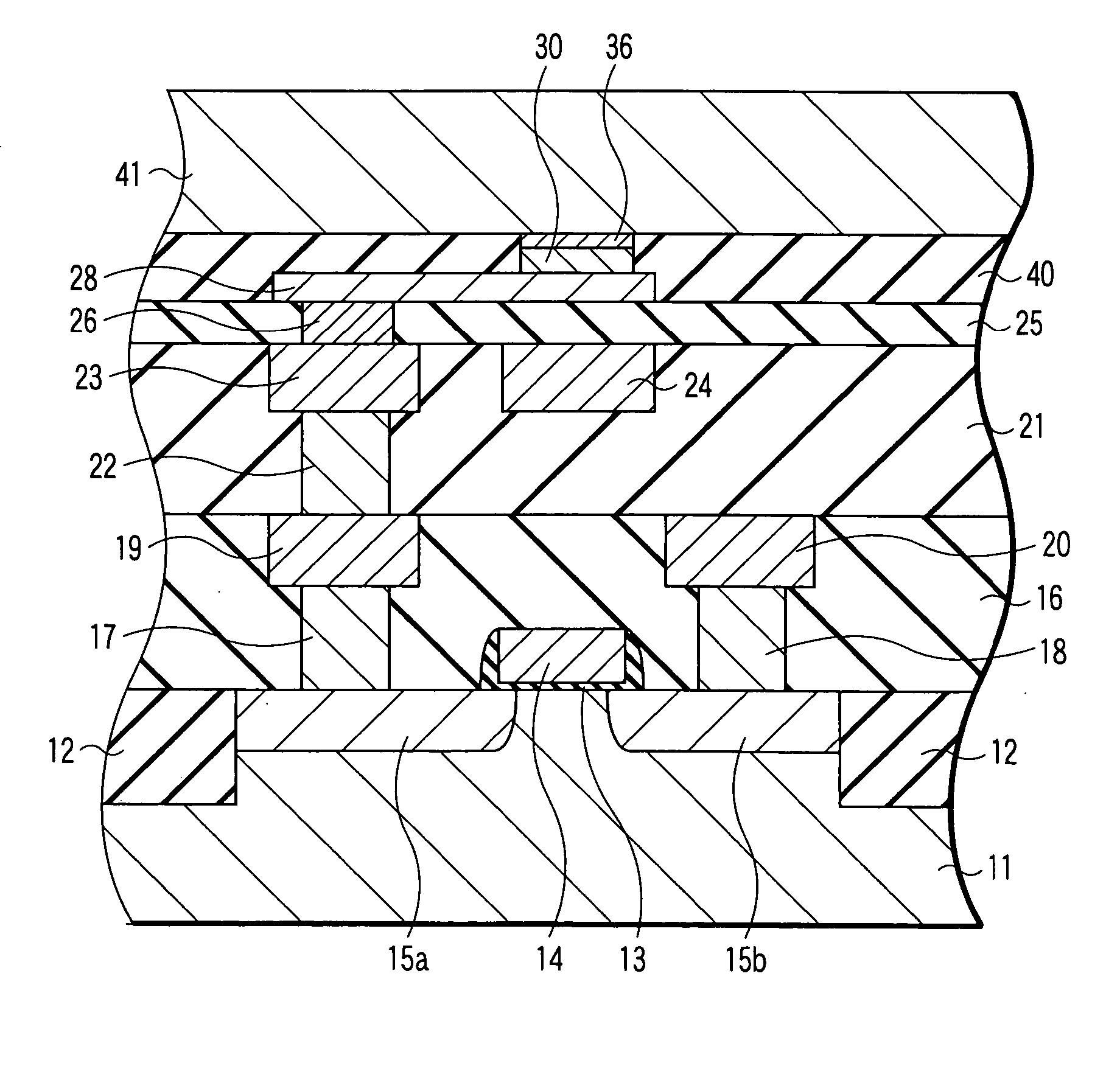
the present invention will now be described with reference to the accompanying drawings. In the description below of the first embodiment, the same or similar structural parts are denoted by like reference numerals and a detailed description is omitted to avoid overlapping description.

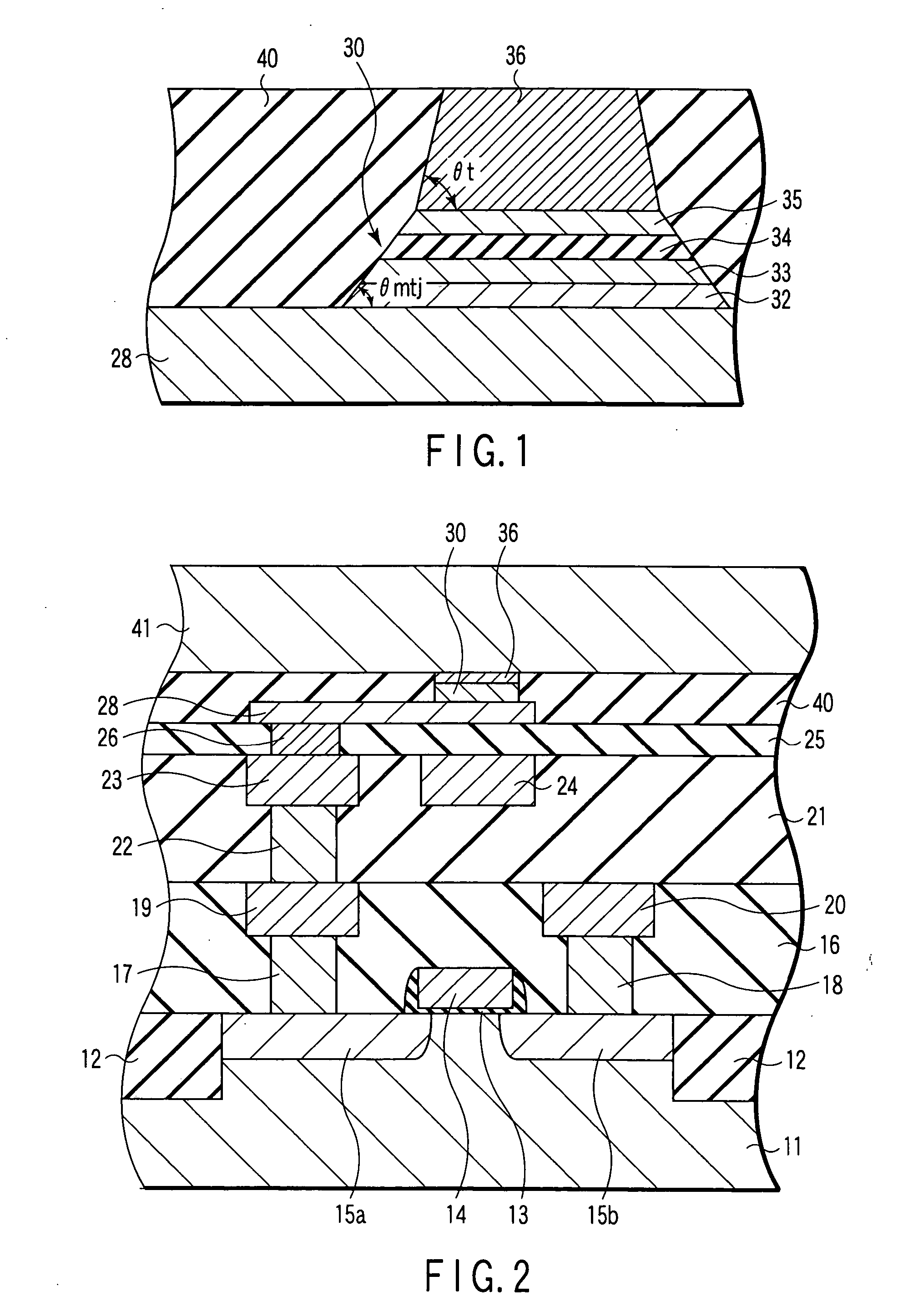
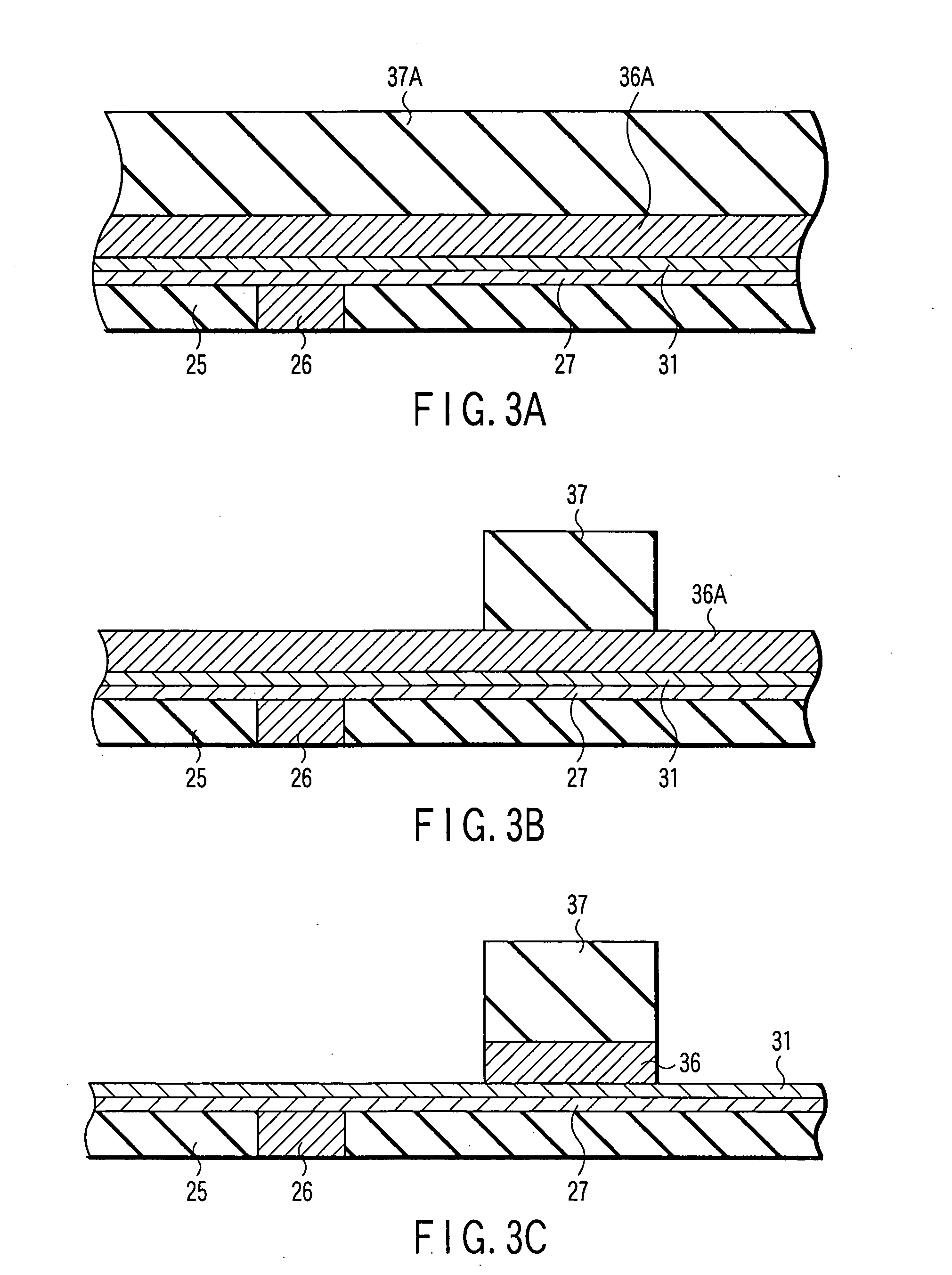
FIG. 1 is a cross-sectional view of an MTJ element 30 formed as a magneto-resistive element according to an embodiment of the invention. In FIG. 1, the MTJ element 30 is formed on a lower electrode 28. A mask (hereinafter referred to as “hard mask”) 36 is formed on the MTJ element 30. An interlayer insulation film 40 is integrally formed to cover the entirety of the lower electrode 28, MTJ element 30 and hard mask 36. The upper surface of the hard mask 36 is flush with the upper surface of the interlayer insulation film 40 and is exposed from the interlayer insulation film 40.

The MTJ element 30 has a four-layer structure. The MTJ element 30 comprises an antiferromagnetic layer 32, a first ferromagnet...


PUM

PropertyMeasurementUnit
taper angleaaaaaaaaaa
angleaaaaaaaaaa
angleaaaaaaaaaa

Abstract

A method of manufacturing a magnetic memory device includes forming an insulation layer on a substrate, forming a lower electrode on the insulation layer, forming a magneto-resistive film on an upper surface of the lower electrode, the magneto-resistive film including an insulation barrier layer and a plurality of magnetic films stacked on both sides of the insulation barrier layer, stacking a mask layer on the magneto-resistive film, performing ion etching on the magneto-resistive film, using the mask layer as a mask, thereby forming a magneto-resistive element, forming an insulation film on upper surfaces of the mask, the magneto-resistive element and the lower electrode, and etching the insulation film with an ion beam such that a side surface of the magneto-resistive element is exposed.

Description

CROSS-REFERENCE TO RELATED APPLICATIONS This application is based upon and claims the benefit of priority from the prior Japanese Patent Application No. 2003-200413, filed Jul. 23, 2003, the entire contents of which are incorporated herein by reference. BACKGROUND OF THE INVENTION 1. Field of the Invention The present invention relates to a magnetic memory device of a magnetic random access memory (hereinafter referred to as “MRAM”), and more particularly to a magnetic memory device using a magneto-resistive element and a method of manufacturing the magnetic memory device. 2. Description of the Related Art The MRAM is a generic term of a nonvolatile solid-state memory which can randomly rewrite, store and read information as an information recording medium, making use of a variation in resistance value of a barrier layer due to a change in direction of magnetization of ferromagnetic layers. In general, a memory cell of the MRAM has a stacked structure of a plurality of ferromag...

Claims


Application Information

Patent Timeline
Patent Type & Authority Applications(United States)
IPC IPC(8): H01L27/105C23F4/00G11C11/00G11C11/02H01F10/32H01F41/30H01L21/336H01L21/8246H01L27/00H01L27/22H01L29/76H01L31/119H01L43/08H01L43/12
CPCB82Y10/00B82Y25/00B82Y40/00C23F4/00H01L43/12H01F41/308H01L27/228H01L43/08H01F10/3254H10B61/22H10N50/10H10N50/01H01L27/105
Inventor NAKAJIMA, KENTAROAMANO, MINORUUEDA, TOMOMASATAKAHASHI, SHIGEKI
Owner KIOXIA CORP
Why Eureka
Try Eureka