Method of preparing a surface of a semiconductor wafer to make it epiready

a technology of epiready and semiconductor wafers, applied in semiconductor devices, manufacturing tools, lapping machines, etc., can solve the problems of incompatibility with epitaxial growth, inability to produce the desired final roughness value (0.1 to 0.2 nm rms) and the lik

Inactive Publication Date: 2005-01-27
SOITEC SA
View PDF6 Cites 26 Cited by
  • Summary
  • Abstract
  • Description
  • Claims
  • Application Information

AI Technical Summary

Problems solved by technology

After detachment, that method results in a roughness value of about 5 nm root mean square (rms), which is not compatible with epitaxial growth.
However, it has been observed that such techniques cannot produce the desired final roughness value (of 0.1 to 0.2 nm rms) for epitaxy on SiC.
The annealing step does not consume sufficient material to significantly reduce the roughness value since thermal SiC oxidation is very slow, especially on the silicon face.
Further, it is difficult to conduct chemical-mechanical polishing (CMP) of SiC since the chemical reactivity of the polished surfaces is low compared with materials such as silicon.
Further, the mechanical hardness of SiC is extremely high and the use of “diamond” abrasives or certain other abrasives that are known for polishing silicon may result in scratches.
Thus, it is difficult to find an abrasive to use which results in a sufficiently high removal rate without creating scratches and defects.
Hence, SiC polishing methods are often very lengthy (several hours).
Further, abrasives based on diamond particles cannot produce the desired roughness of less than 1 nm rms.
Such techniques are of interest concerning the removal rates, but the surface condition is often too rough for epitaxy, and in particular, the surface cannot be easily smoothed.

Method used


Image

  • Method of preparing a surface of a semiconductor wafer to make it epiready
  • Method of preparing a surface of a semiconductor wafer to make it epiready

Examples


example

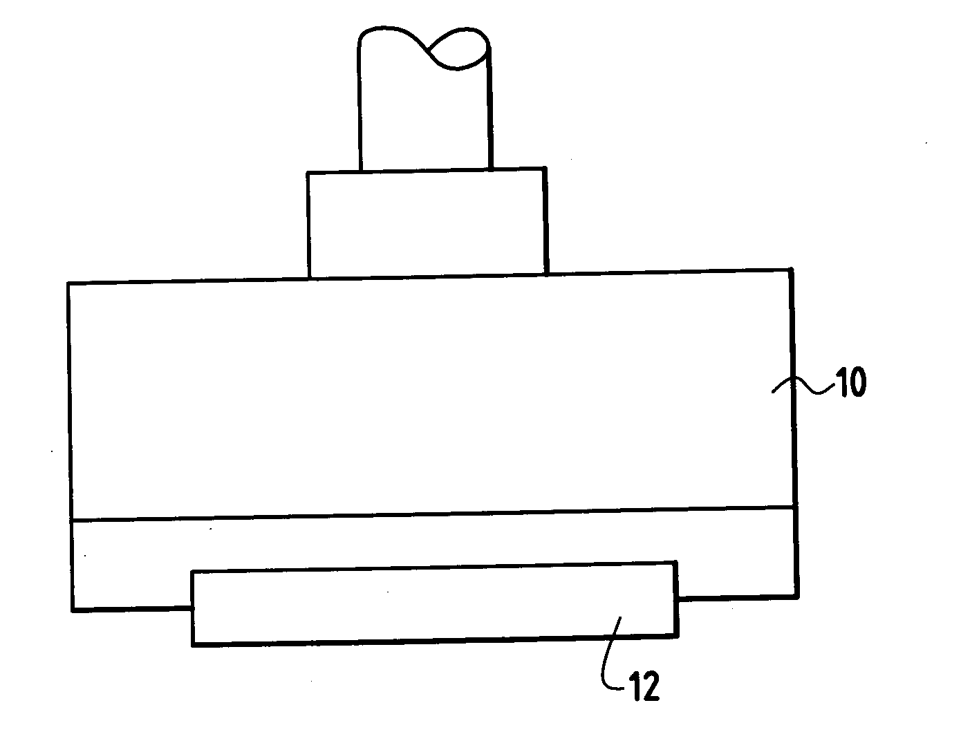
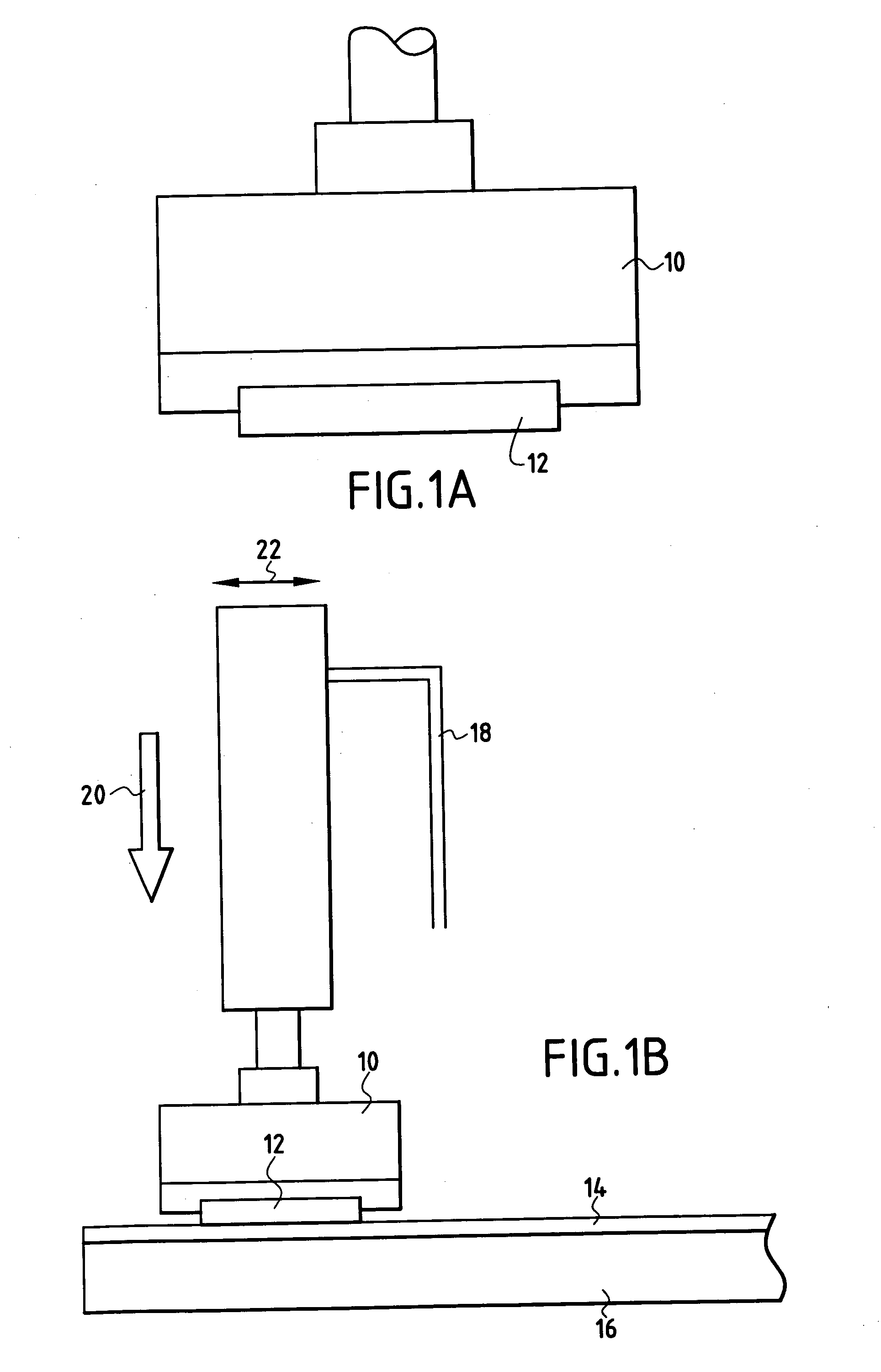
[0020] The following is an example relating to a thin film of a 4H type SiC (obtained by the SMART-CUT® method). An annealing step was carried out in an oxidizing atmosphere (for example, for 2 hours at 1150° C.), followed by surface deoxidation in 10% HF followed by polishing the surface by CMP. Polishing was carried out with the use of a rotating polishing plate onto which a polishing head had been applied, also rotating, the speed of rotation being of the order of 60 revolutions per minute (rpm) with a pressure of 0.75 bars applied to the head. The pad used was a “hard” type IC1000 pad distributed by the RODEL company, with a slurry which was a SYTON W30-type colloidal silica.

[0021] The polishing time was about 15 minutes (min) to about 30 min, and the roughness obtained after polishing was on the order of about 3 Å rms. Final cleaning carried out using deionized water with a 10% HF bath for 10 minutes.

[0022] Table I below summarizes the results obtained for thin SiC films unde...


PUM

PropertyMeasurementUnit
temperatureaaaaaaaaaa
pressureaaaaaaaaaa
surface roughnessaaaaaaaaaa

Abstract

The invention concerns a method of preparing the surface of a semiconductor wafer intended for microelectronics and / or optoelectronics applications. In particular, a method of preparing a SiC surface of a semiconductor wafer to make it epiready is described. The technique includes annealing the wafer in an oxidizing atmosphere, and polishing a surface of the wafer with an abrasive based on particles of colloidal silica to make the SiC wafer surface suitable for homoepitaxy or heteroepitaxy.

Description

BACKGROUND ART [0001] The present invention generally relates to the treatment of semiconductor materials intended for microelectronics and / or optoelectronics applications. In particular, it relates to a method of preparing the surface of a thin film having a thickness in the range of about 1 nanometer (nm) or a few tens of nm to about 100 nm or a few hundred nm, for example 400 nm or 500 nm. More particularly, the invention relates to preparing the surface of a film of monocrystalline silicon carbide so that it is “epiready”, meaning that the surface is ready for epitaxy, i.e., to receive growth of an epitaxial film thereon. In an implementation, the film may be a silicon carbide film transferred onto a further material (silicon, monocrystalline or polycrystalline SiC covered with an oxide or other film such as deposited oxide, nitride, etc). [0002] In order to obtain good quality epitaxy, the starting surface must be free of defects and must be as smooth as possible. A thin layer ...

Claims


Application Information

Patent Timeline
Patent Type & Authority Applications(United States)
IPC IPC(8): B24B37/04H01L21/04
CPCB24B37/042H01L21/02024H01L21/02378H01L21/0243Y10S438/931H01L21/0254H01L21/02658H01L29/1608H01L21/02529B24B37/04B24B37/10H01L21/304
Inventor RICHTARCH, CLAIRE
Owner SOITEC SA
Why Eureka
Try Eureka