Crack stop for low k dielectrics

a dielectric material and crack stop technology, applied in the direction of electrical equipment, semiconductor devices, semiconductor/solid-state device details, etc., can solve the problem that the addition of edge seals has the disadvantage of taking up more area on the ic chip, and achieve the effect of preventing the propagation of cracks

Inactive Publication Date: 2005-02-03
GLOBALFOUNDRIES INC
View PDF19 Cites 99 Cited by
  • Summary
  • Abstract
  • Description
  • Claims
  • Application Information

AI Technical Summary

Benefits of technology

[0009] The present invention provides crack stop structures, and methods for forming crack stop structures, for an integrated circuit (IC) formed on an IC chip using metal interconnects which do not form a self-passivating oxide layer, such as copper or silver interconnects, in a low-K dielectric material such as silicon dioxide SiO2. The crack stop prevents the propagation of cracks, caused by chipping and cracking formed along peripheral edges of the IC chip during a dicing operation, into active circuit areas of the IC chip. A moisture barrier or edge seal is formed as a metal stack positioned along the outer peripheral edges of the active area of the IC chip. The crack stop is formed by at least one trench or groove positioned outside of the moisture barrier / edge seal on the outer periphery of the IC chip.

Problems solved by technology

During an IC chip dicing operation, cracks form that can propagate into the active area of the IC chip, causing fails.
However the additional edge seal has the disadvantage of taking up more area on the IC chip.

Method used


Image

  • Crack stop for low k dielectrics
  • Crack stop for low k dielectrics
  • Crack stop for low k dielectrics

Examples


Embodiment Construction

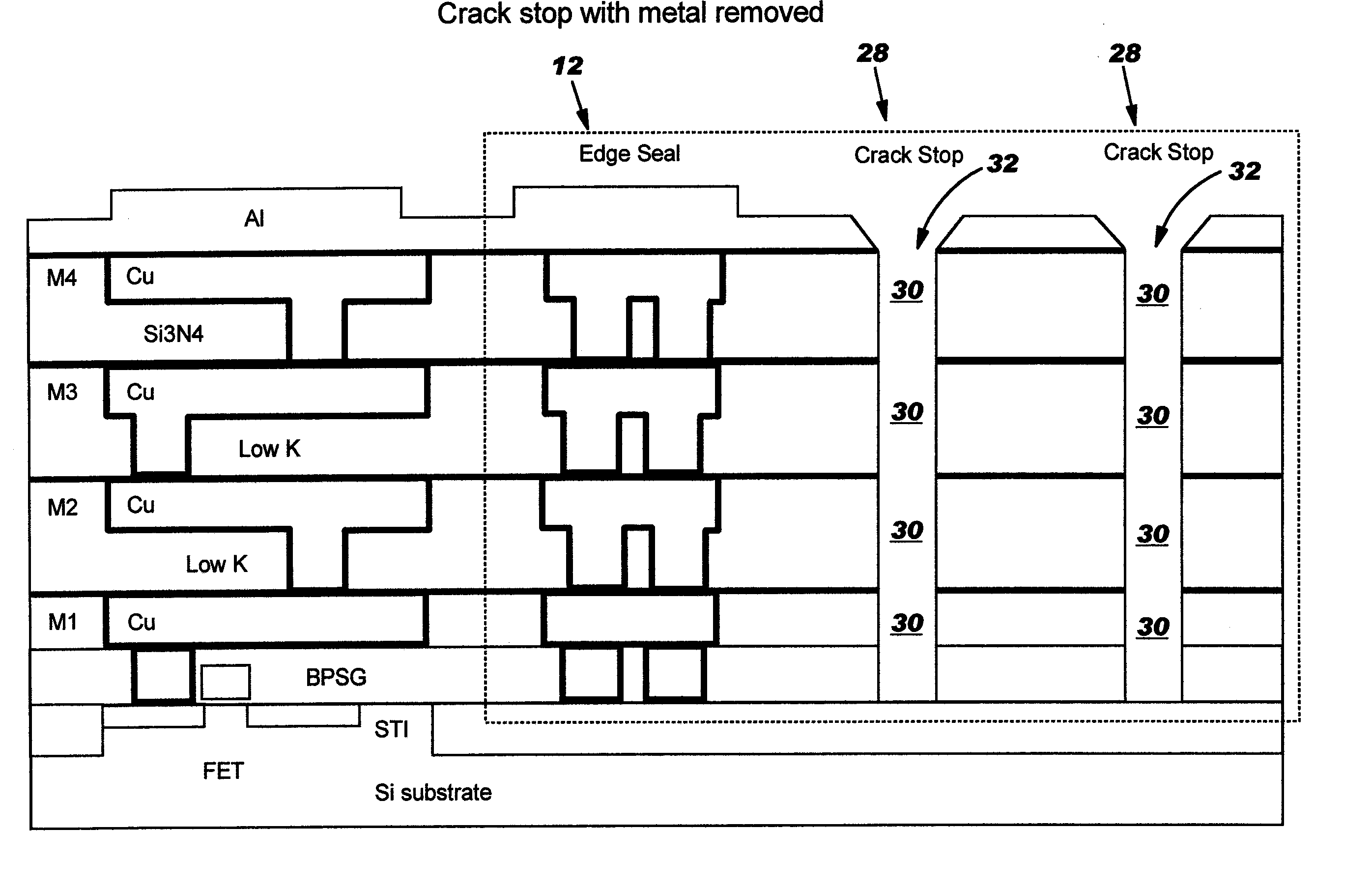
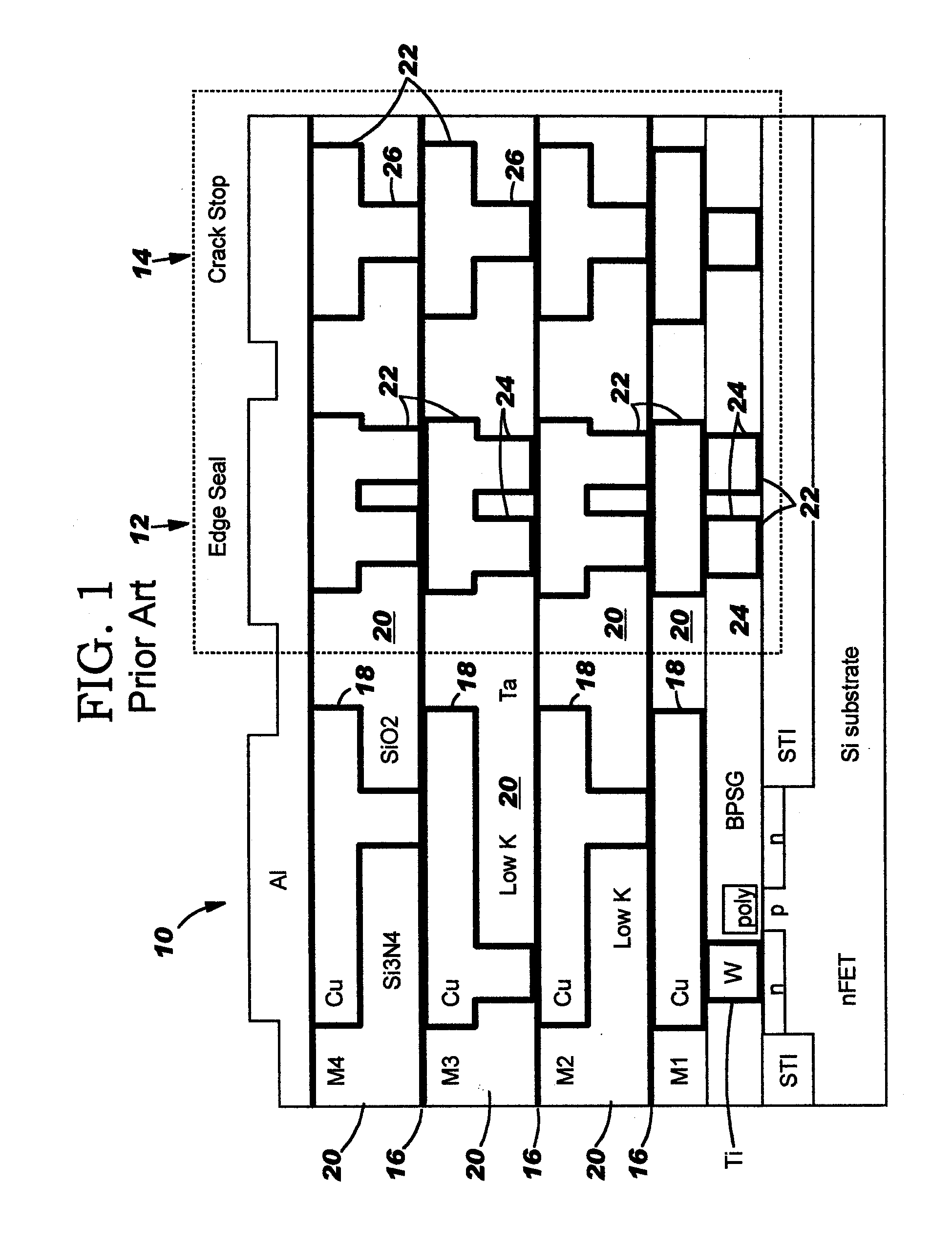
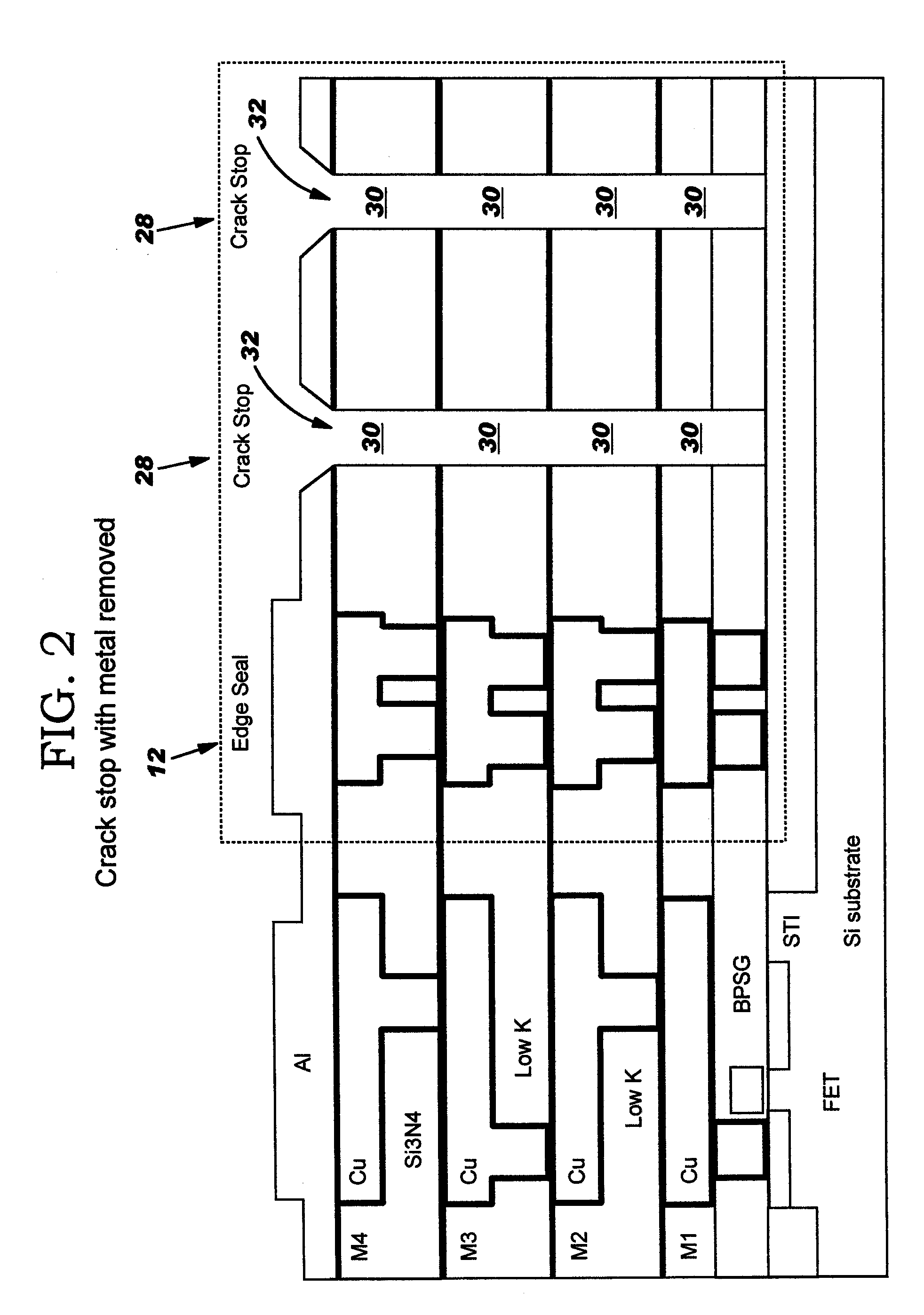
[0014]FIG. 1 illustrates a prior art metal stack crack stop which has been used in copper interconnect technology on IC chips to prevent the propagation of cracks formed during dicing of the IC chip into brittle BEOL dielectrics of the IC chip. The active circuit area 10 of the IC chip is formed generally to the left in FIG. 1, and is bordered by a moisture barrier / edge seal 12 formed along its outer peripheral edge, and a metal stack crack stop 14 formed outside of the edge seal.

[0015] The IC chip is formed on a silicon Si substrate, and an exemplary active area of the IC chip is shown on the left side of FIG. 1. The exemplary active area includes an npn nFET transistor device surrounded by shallow trench isolation STI, with a poly conductor above the p gate, a titanium Ti or TiN liner formed around tungsten W above the left n region, and a layer of BPSG (borophospho silicate glass) above the right n region. The active area includes metal layers M1, M2, M3, M4, separated by cappin...


PUM


Abstract

A crack stop for low K dielectric materials of an integrated circuit (IC) formed on an IC chip using metal interconnects which do not form a self-passivating oxide layer, such as copper or silver interconnects, in a low-K dielectric material to prevent damage to the active area of the IC chip caused by chipping and cracking formed along peripheral edges of the IC chip during a dicing operation. A moisture barrier or edge seal is formed as a metal stack positioned along the outer peripheral edges of the active area of the IC chip. The crack stop is formed by at least one trench or groove positioned outside of the moisture barrier / edge seal on the outer periphery of the IC chip.

Description

BACKGROUND OF INVENTION [0001] 1. Field of the Invention [0002] The present invention relates generally to a crack stop for low K dielectric materials of an integrated circuit (IC) formed on an IC chip using metal interconnects which do not form a self-passivating oxide layer, such as copper or silver interconnects, in a low-K dielectric material such as silicon dioxide SiO2. [0003] More particularly, the subject invention pertains to crack stop structures, and methods for forming the crack stop structures, for preventing damage to the active area of an IC chip, using metal interconnects such as copper or silver interconnects in a low-K dielectric material, caused by chipping and cracking formed along peripheral edges of the IC chip during a dicing operation performed on the IC chip. A moisture barrier or edge seal is formed as a metal stack positioned along the outer peripheral edges of the active area of the IC chip. The crack stop is formed by at least one trench or groove positi...

Claims


Application Information

Patent Timeline
Patent Type & Authority Applications(United States)
IPC IPC(8): H01LH01L21/301H01L21/311H01L21/3213H01L21/78H01L23/00H01L23/28H01L23/58
CPCH01L21/31111H01L21/32134H01L21/76838H01L21/78H01L23/562H01L2924/0002H01L23/585H01L2924/00H01L23/28
Inventor DAUBENSPECK, TIMOTHY H.GAMBINO, JEFFREY P.LUCE, STEPHEN E.MCDEVITT, THOMAS L.MOTSIFF, WILLIAM T.POULIOT, MARK J.ROBBINS, JENNIFER C.
Owner GLOBALFOUNDRIES INC
Why Eureka
Try Eureka