Method of fabricating cylindrical bonding structure

a cylindrical bonding and structure technology, applied in the direction of electrical equipment, semiconductor devices, semiconductor/solid-state device details, etc., can solve the problems of low overall yield of the flip-chip package, bad electrical connection etc., to reduce the separation between neighboring bonding pads, improve the reliability of the junction and increase the separation distance between the chip and the substra

Inactive Publication Date: 2005-02-03
QUALCOMM INC
View PDF12 Cites 57 Cited by
  • Summary
  • Abstract
  • Description
  • Claims
  • Application Information

AI Technical Summary

Benefits of technology

[0012] Accordingly, one object of the present invention is to provide a cylindrical bonding structure and its method of manufacture capable of reducing the separation between neighboring bonding pads on a chip while increasing distance of separation between the chip and a substrate. Ultimately, reliability of the junctions connecting the chip and the substrate is improved and post-packaging life of the chip is extended.

Problems solved by technology

Poor adhesion often leads to bad electrical connections between the chip and the substrate and a low overall yield of the flip chip package.

Method used


Image

  • Method of fabricating cylindrical bonding structure
  • Method of fabricating cylindrical bonding structure
  • Method of fabricating cylindrical bonding structure

Examples


first embodiment

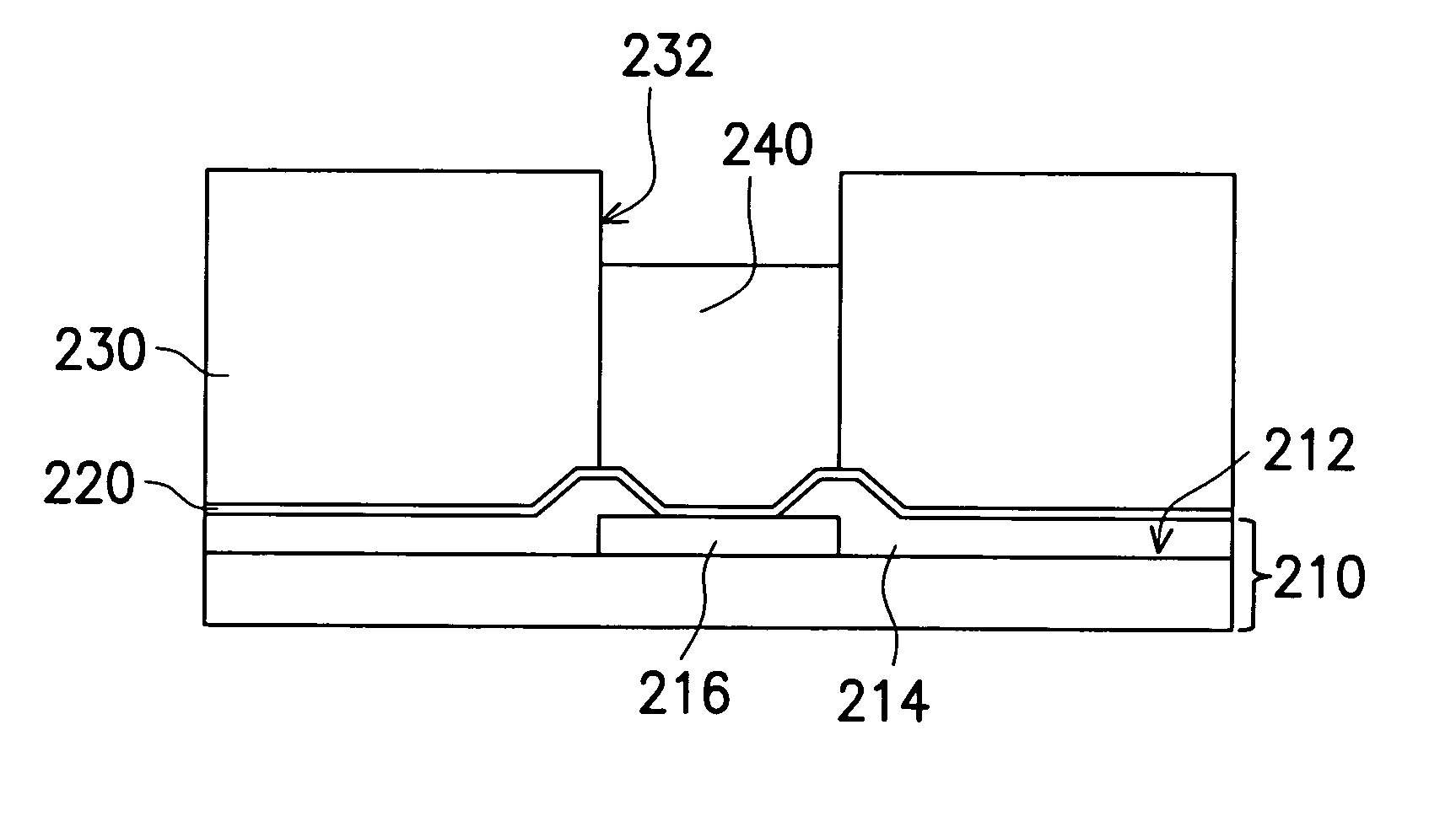
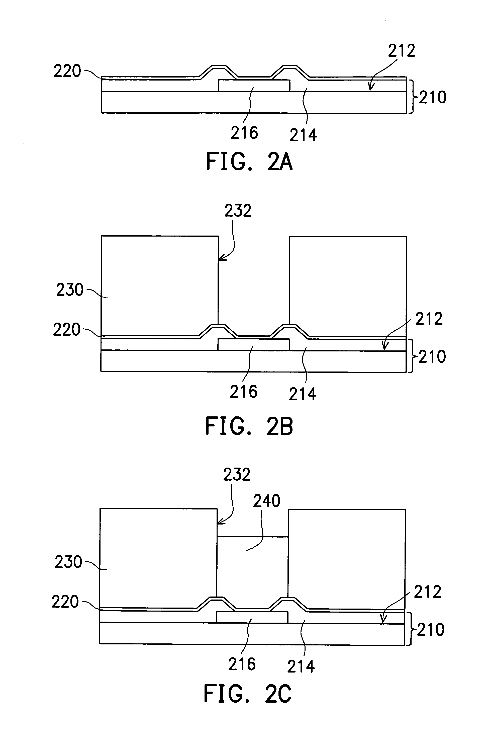
[0030] FIGS. 2A˜2F are schematic cross-sectional views showing the progression of steps for producing a cylindrical bonding structure according to this invention. As shown in FIG. 2A, a silicon wafer 210 is provided. Since each chip (not shown) is formed by cutting up the wafer 210 and any redistribution layer or bumps are formed before cutting, the wafer 210 actually represents a congregation of uncut chips. Furthermore, the active surface 212 of the wafer 210 has a passivation layer 214 and a plurality of bonding pads 216 (only one bonding pad is shown in FIG. 2A). The active surface 212 of the wafer 210 refers to the side of the wafer 210 where active devices are formed. The patterned passivation layer 214 exposes the bonding pads 216. Note that bonding pads 216 includes those original pads on the chips or the bonding pads of any redistribution circuit layer on the chips. The purpose of having a redistribution layer is to relocate the original bonding pads on the chip to some oth...

third embodiment

[0050] FIGS. 5A˜5C are schematic cross-sectional views showing an application of the third cylindrical bonding structure according to this invention to the fabrication of a flip-chip package. As shown in FIG. 5A, a cylindrical bonding structure 514 according to this invention is formed on the bonding pad 512 of a chip 510. The cylindrical bonding structure 514 comprises a ball contact metallic layer 514a, a conductive pillar 514b and a cylindrical solder cap 514c. In addition, a substrate 520 having a solder mask layer 524 and a pad 522 thereon is also provided. The solder mask 524 has a plurality of openings 526 that exposes the pads 522. In one aspect, the solder cap 514c has a transverse length w1 smaller than the corresponding transverse length w2 of the opening 526 in the solder mask layer 524 of the substrate 520. In one aspect, the solder cap 514c has a length D1 greater than the corresponding depth D2 of the opening 526 in the solder mask layer 524 of the substrate 520.

[0051...


PUM


Abstract

A cylindrical bonding structure and its method of manufacture. The cylindrical bonding structure is formed over the bonding pad of a silicon chip and the chip is flipped over to connect with a substrate board in the process of forming a flip-chip package. The cylindrical bonding structure mainly includes a conductive pillar and a solder cap. The conductive pillar is formed over the bonding pad of the silicon chip and the solder cap is attached to the upper end of the conductive pillar. The solder cap has a melting point lower than the conductive pillar. The solder cap can be configured into a cylindrical, spherical or hemispherical shape. To fabricate the cylindrical bonding structure, a patterned mask layer having a plurality of openings that correspond in position to the bonding pads on the wafer is formed over a silicon wafer. Conductive material is deposited into the openings to form conductive pillars and finally a solder cap is attached to the end of each conductive pillar.

Description

CROSS-REFERENCE TO RELATED APPLICATION [0001] This application is a Continuation-In-Part of Ser. No. 10 / 174,357 filed on Jun. 17, 2002, which is a divisional application of Ser. No. 10 / 055,580 filed on Jan. 22, 2002.BACKGROUND OF THE INVENTION [0002] 1. Field of Invention [0003] The present invention relates to a cylindrical bonding structure and its method of manufacture. More particularly, the present invention relates to a cylindrical bonding structure for a flip chip package and a method of fabricating the cylindrical bonding structure. [0004] 2. Description of Related Art [0005] In this information-saturated society, working with electronic products has become an integral part of our daily life. Currently, integrated circuit products are used for doing business, educating our children or providing us with games for recreation. As a result of rapid progress in electronic technologies, devices having powerful functions and personalized designs have been developed. Moreover, most ...

Claims


Application Information

Patent Timeline
Patent Type & Authority Applications(United States)
IPC IPC(8): H01L21/60H01L21/98H01L23/485H01L25/065
CPCH01L24/11H01L2924/0002H01L25/50H01L2224/11462H01L2224/1147H01L2224/11849H01L2224/13099H01L2224/13609H01L2224/16145H01L2225/06513H01L2924/01012H01L2924/01022H01L2924/01027H01L2924/01029H01L2924/0103H01L2924/01046H01L2924/01047H01L2924/01049H01L2924/01051H01L2924/01074H01L2924/01078H01L2924/01079H01L2924/01082H01L2924/14H01L2224/1308H01L2224/13123H01L24/13H01L2224/13083H01L2224/13109H01L2224/13111H01L2224/13113H01L2224/13116H01L2224/13118H01L2224/1312H01L2224/13139H01L2224/13144H01L2224/13147H01L2224/13155H01L2924/00013H01L2924/01005H01L2924/01006H01L2924/01023H01L2924/01024H01L2924/01033H01L2924/01073H01L2924/014H01L2924/04953H01L2224/11474H01L25/0657H01L2224/0401H01L2924/10253H01L2224/81191H01L2224/16237H01L2224/05572H01L2924/00014H01L2224/29099H01L2924/00H01L2224/05552H01L2224/11906H01L2224/05611H01L2224/05639H01L2224/05644H01L2224/05647H01L2224/05655H01L2224/05664H01L2224/05666H01L2224/05671H01L2224/05684H01L2224/05657H01L2224/05672H01L2224/13022H01L2224/13017H01L24/05H01L24/03H01L2924/013
Inventor LEE, JIN-YUANCHOU, CHIEN-KANGLIN, SHIH-HSIUNGKUO, HSI-SHAN
Owner QUALCOMM INC
Why Eureka
Try Eureka