Input device, electronic apparatus, and method for driving input device

a technology of input device and electronic apparatus, which is applied in the field of input devices, can solve the problems of high energy and labor, poor durability of the related art capacitive fingerprint sensor, and large amount of energy and labor, and achieve the effect of small and lightweight input device and reduced power consumption

Inactive Publication Date: 2005-02-10
SEIKO EPSON CORP
View PDF22 Cites 86 Cited by
  • Summary
  • Abstract
  • Description
  • Claims
  • Application Information

AI Technical Summary

Benefits of technology

[0008] In view of the issues and factors described above, the present invention provides an input device, an electronic apparatus, and a method for driving an input device that still restrict an increase in the amount of processed information to make the processing system simple.
[0011] According to an aspect of the present invention, at least two field scans are performed on the plurality of sensor cells arranged in an m-row×n-column matrix. The detected information is used to identify particular sensor cells from among all sensor cells. Various processing is performed based on the detected information only from these identified sensor cells. Thus, the amount of processed information is minimized, and therefore processing systems can be made simple.
[0017] According to an aspect of the present invention, it is possible to more accurately identify the particular sensor cells by comparing the detected information read from all sensor cells with the predetermined threshold.
[0020] According to an aspect of the present invention, in the second and the subsequent field scans, only the scanning lines corresponding to the particular sensor cells are selected and scanned and then detected information is read by connecting only corresponding data lines to an output device. Thus, an operation associated with scanning of the sensor cells, other than the particular sensor cells and the reading of detected information from the data lines corresponding to the sensor cells, is prevented to reduce the power consumption associated with the driving of the sensor cells.
[0023] According to an aspect of the present invention, all scanning lines are sequentially scanned in the second and the subsequent field scans. In this case, however, the scanning lines corresponding to the sensor cells from which detected information is not read are scanned at a higher speed than that of the scanning lines corresponding to the sensor cells from which detected information is read. In this manner, detected information is read from the data lines corresponding to the particular sensor cells. Thus, unnecessary operation associated with scanning of the sensor cells and the reading of detected information from the data lines is prevented to reduce the power consumption associated with the driving of the sensor cells.
[0024] In the above-described aspects of the present invention, the sensor cells can detect various types of physical quantity. The sensor cells may be applied particularly to a fingerprint sensor to detect ridges and valleys of a fingerprint. This allows for various controls with the fingerprint information as detected information. When a fingerprint sensor to output fingerprint information is used, an extremely small and lightweight input device can be provided.

Problems solved by technology

Unfortunately, these related art capacitive fingerprint sensors have sensor electrodes and dielectric films formed on a single-crystal silicon substrate, which may break if a finger is strongly pressed onto the dielectric films, that is, the detection surface.
In short, the durability of the related art capacitive fingerprint sensors is poor.
This requirement causes the fingerprint sensor to become expensive when it is formed on a single-crystal silicon substrate which requires a huge amount of energy and labor to produce.
For this reason, if authentication is performed by reading fingerprint information from all sensor cells, a processing system for the fingerprint authentication becomes complicated due to an increase in the amount of processed information.

Method used


Image

  • Input device, electronic apparatus, and method for driving input device
  • Input device, electronic apparatus, and method for driving input device
  • Input device, electronic apparatus, and method for driving input device

Examples


first exemplary embodiment

[0040] First Exemplary Embodiment

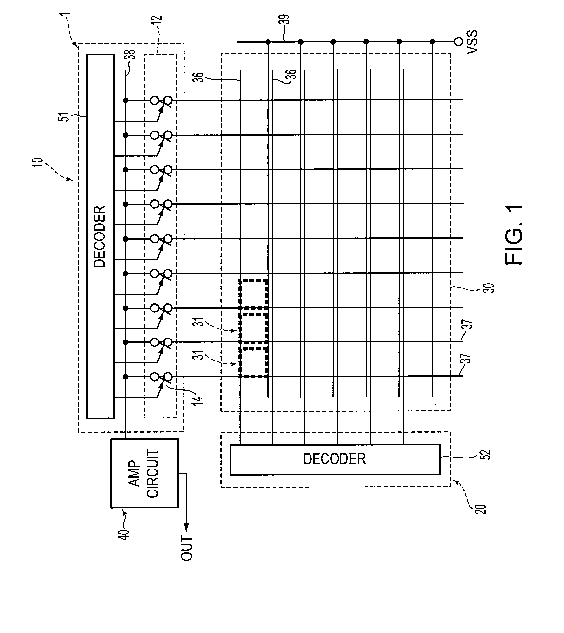
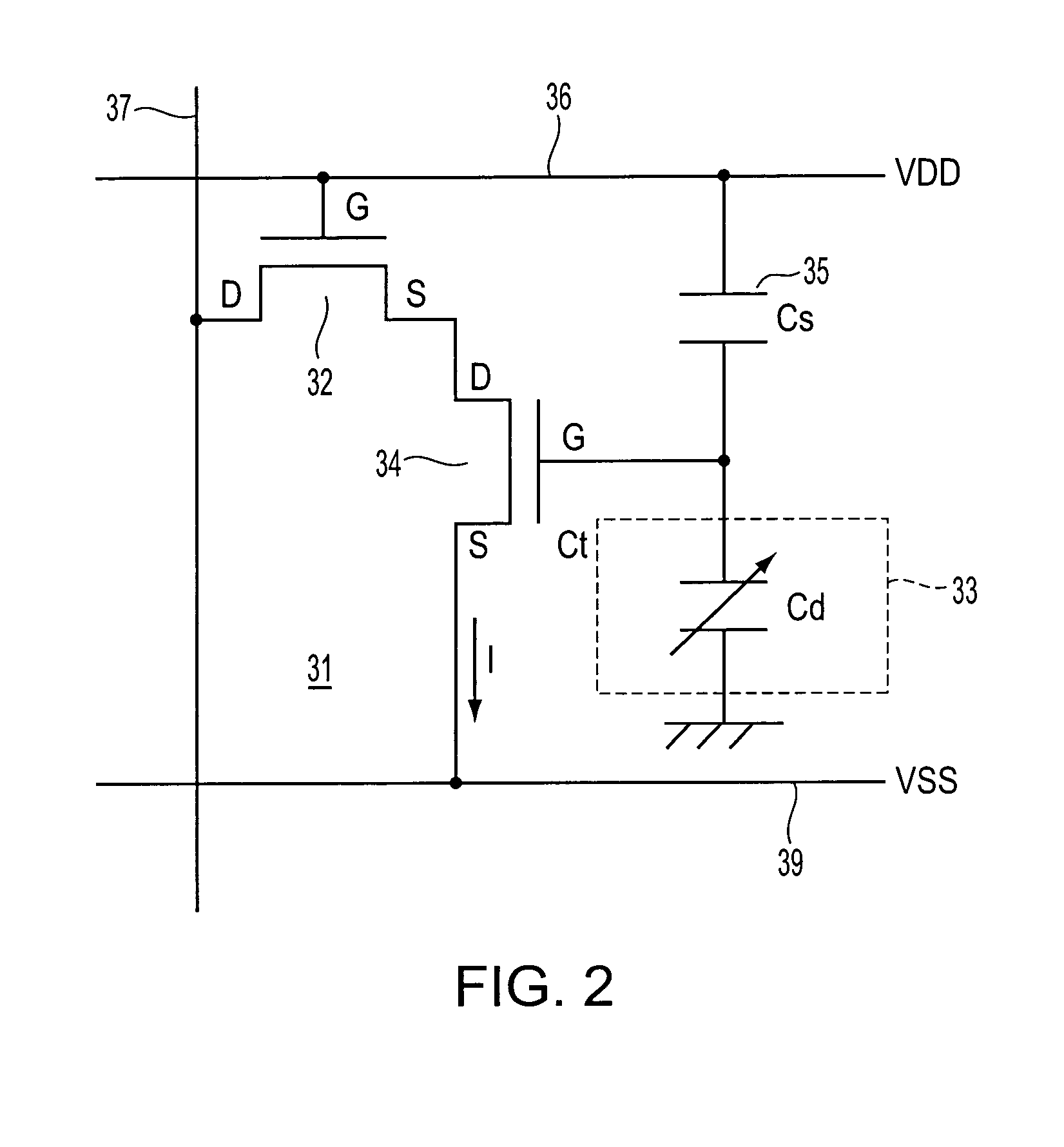
[0041]FIG. 1 is a schematic of a capacitive fingerprint sensor 1, which functions as a sensor section of an input device. The fingerprint sensor 1 includes a data driver 10 to select data lines 37, a scan driver 20 to select scanning lines 36, an active matrix 30 formed as a detection area of a detection object, such as a fingerprint, and an amp circuit 40 to amplify a detection signal from the active matrix 30. The active matrix 30, which functions as an information-collecting section to collect the pattern of the surface of a finger, includes the m (two or larger integer) scanning lines 36 and the n (two or larger integer) data lines 37 arranged in an m-row×n-column matrix and capacitive sensing circuits 31 corresponding to the sensor cells provided at the intersections between the scanning lines 36 and the data lines 37. Each of the capacitive sensing circuits 31 has a supply line 39 connected to a low-voltage power supply (not shown in the figure...

second exemplary embodiment

[0083] Second Exemplary Embodiment

[0084]FIG. 9 is a schematic of a capacitive fingerprint sensor 1 according to a second exemplary embodiment of the present invention. In this exemplary embodiment, a shift register 11 to sequentially drive analog dots of a typical display apparatus is provided in the data driver 10 in place of the data decoder 51 described above. Furthermore, the scan driver 20 is provided with a shift register 21 to sequentially select the scanning lines 36 in place of the scan decoder 52. Upon receiving an external start pulse, the shift register 11 sequentially selects and scans all scanning lines 36 in synchronization with another applied clock. The components of the fingerprint sensor 1, other than those described above, including the capacitive sensing circuits 31 and the circuit structure of the amp circuit 40, are the same as in the first exemplary embodiment.

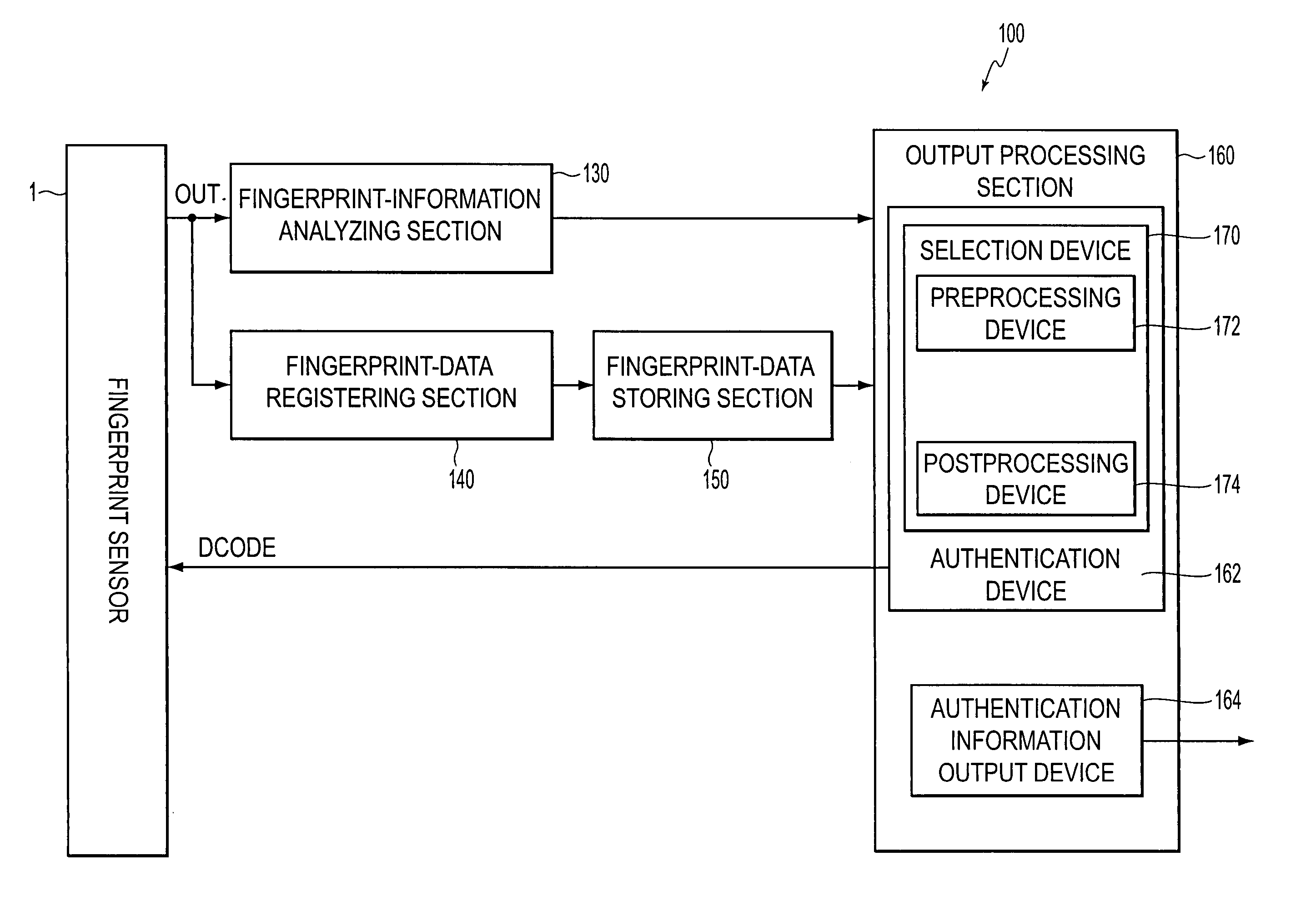
[0085]FIG. 10 is a schematic of the structure of an input device. In place of the output line for t...


PUM


Abstract

To provide an input device, an electronic device, and a method for driving an input device where an increase in the amount of processed information is restricted to make processing systems simple, an input device includes a plurality of capacitive sensing circuits arranged in a matrix and an amp circuit to output detected information from the capacitive sensing circuits. An output processing section performs a plurality of field scans to read fingerprint information from the capacitive sensing circuits and thereby identify particular capacitive sensing circuits to acquire detected information necessary for processing.

Description

BACKGROUND OF THE INVENTION [0001] 1. Field of Invention [0002] The present invention relates to input devices. In particular, the present invention relates to an input device having sensor cells arranged in a matrix, an electronic apparatus, and a method for driving an input device. [0003] 2. Description of Related Art [0004] Typical input devices having sensor cells arranged in a matrix include a fingerprint sensor (see, Japanese Unexamined Patent Application Publication No. 11-118415, Japanese Unexamined Patent Application Publication No. 2000-346608, Japanese Unexamined Patent Application Publication No. 2001-56204, and Japanese Unexamined Patent Application Publication No. 2001-133213), a seat pressure sensor to measure the pressure distribution on a chair, etc. Fingerprint sensors have mainly been used in a system for authenticating individuals who wish to enter a highly restricted room. Recent capacitive fingerprint sensors with semiconductors (see, Japanese Unexamined Patent...

Claims


Application Information

Patent Timeline
Patent Type & Authority Applications(United States)
IPC IPC(8): G06F3/03G06K9/00G01B7/28G06T1/00
CPCG06K9/0002G06V40/1306G06F3/03
Inventor HARA, HIROYUKISAKURAI, MIKIO
Owner SEIKO EPSON CORP
Why Eureka
Try Eureka