Module for an analysis device, applicator as an exchange part of the analysis device and analysis device associated therewith

a module and analysis device technology, applied in the field of modules for analysis devices, can solve the problems of large waste of valuable si chip area, difficult to reliably separate electrical contact from fluidics, and most chemical-biological developments that have not reached the laboratory trial stage, etc., and achieve the effect of efficient heat transfer and very rapid setting

Inactive Publication Date: 2005-02-10
SIEMENS AG
View PDF6 Cites 199 Cited by
  • Summary
  • Abstract
  • Description
  • Claims
  • Application Information

AI Technical Summary

Benefits of technology

[0010] In the case of a module according to the invention, it is particularly advantageous that the chip carrier is thin and has a thickness of <100 μm. With thicknesses of about 50 μm of metal in combination with about 100 μm of plastic, a considerable volume / material saving is obtained. On account of the thin formation of the chip carrier and suitable material, such as for example gold-coated copper layers, only small masses, and consequently low heat capacities, are obtained, so that, in combination with the good thermal conductivity of silicon and for example a copper / gold layer about 50 μm thick, a very good dynamic thermal behavior results. The processing of the chip carrier takes place on a strip which is transported from reel to reel (“reel to reel” process), it being advantageously possible for the electrical contacting points to be arranged on the rear side.
[0012] Following mounting, wire bonding and encapsulation of the chips on the strip, the sensitive areas of the chips may be coated with chemical / biochemical substances, advantageously from the liquid phase, by a “reel to reel” technique. The encapsulation of the individual module in combination with the associated applicator produces particularly favorable properties.
[0016] For practical purposes, a particularly advantageous embodiment, that is the chip card, comes into consideration as the applicator. In the case of the chip card, the Si chip is mounted on the carrier, which—as already mentioned—is made from a gold-coated copper layer only approximately 50 μm thick. This is the middle metal zone of known chip card modules, which is not used there for electrical contacting points in the card reader. This free zone can consequently be used in the card reader, which serves as an evaluation device, for contacting in particular a cooling element, for example a Peltier cooler, to the corresponding location of the chip card. On account of the placement of the 50 μm thick metallic contact with respect to the chip, an efficient heat transfer is consequently possible, so that a defined temperature can be set very quickly.
[0017] It is particularly advantageous in the case of the invention that the housing concept for realizing the microfluidics is based as much as possible on those of classic microelectronics. This creates the main prerequisites that allow modules with chemical-biological sensors or sensor systems of this type to have commercial success even in the case of relatively small numbers of units.

Problems solved by technology

However, while physical concepts, such as for example pressure and acceleration sensors / systems, have gone through the process of implementation in terms of technical production and successful introduction on the market, most chemical-biological developments have not got beyond the laboratory trial stage.
Consequently, a large part of the valuable Si chip area is wasted.
What is more, the electrical contacting in the housing is located on the same side as the sensitive areas of the chip, which makes it more difficult for the electrical contacting to be reliably separated from the fluidics.
On account of the high development and production costs for comparatively low numbers of units of chemical-biological systems, market penetration of these products is problematical.

Method used


Image

  • Module for an analysis device, applicator as an exchange part of the analysis device and analysis device associated therewith
  • Module for an analysis device, applicator as an exchange part of the analysis device and analysis device associated therewith
  • Module for an analysis device, applicator as an exchange part of the analysis device and analysis device associated therewith

Examples


Embodiment Construction

[0029] Reference will now be made in detail to the preferred embodiments of the present invention, examples of which are illustrated in the accompanying drawings, wherein like reference numerals refer to like elements throughout.

[0030] The drawings, in particular FIGS. 1 and 2, are partly described together.

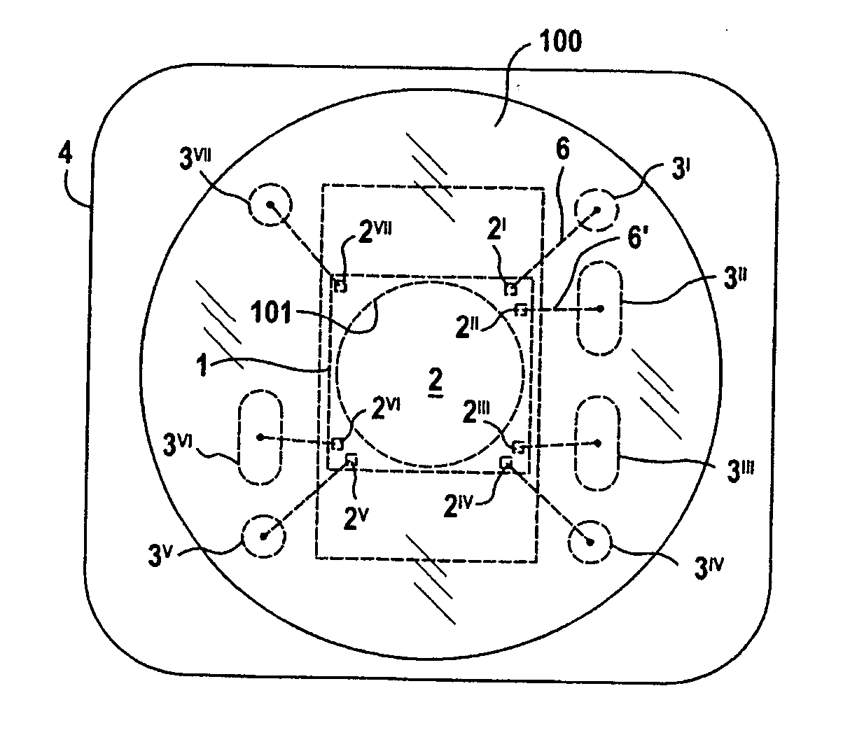
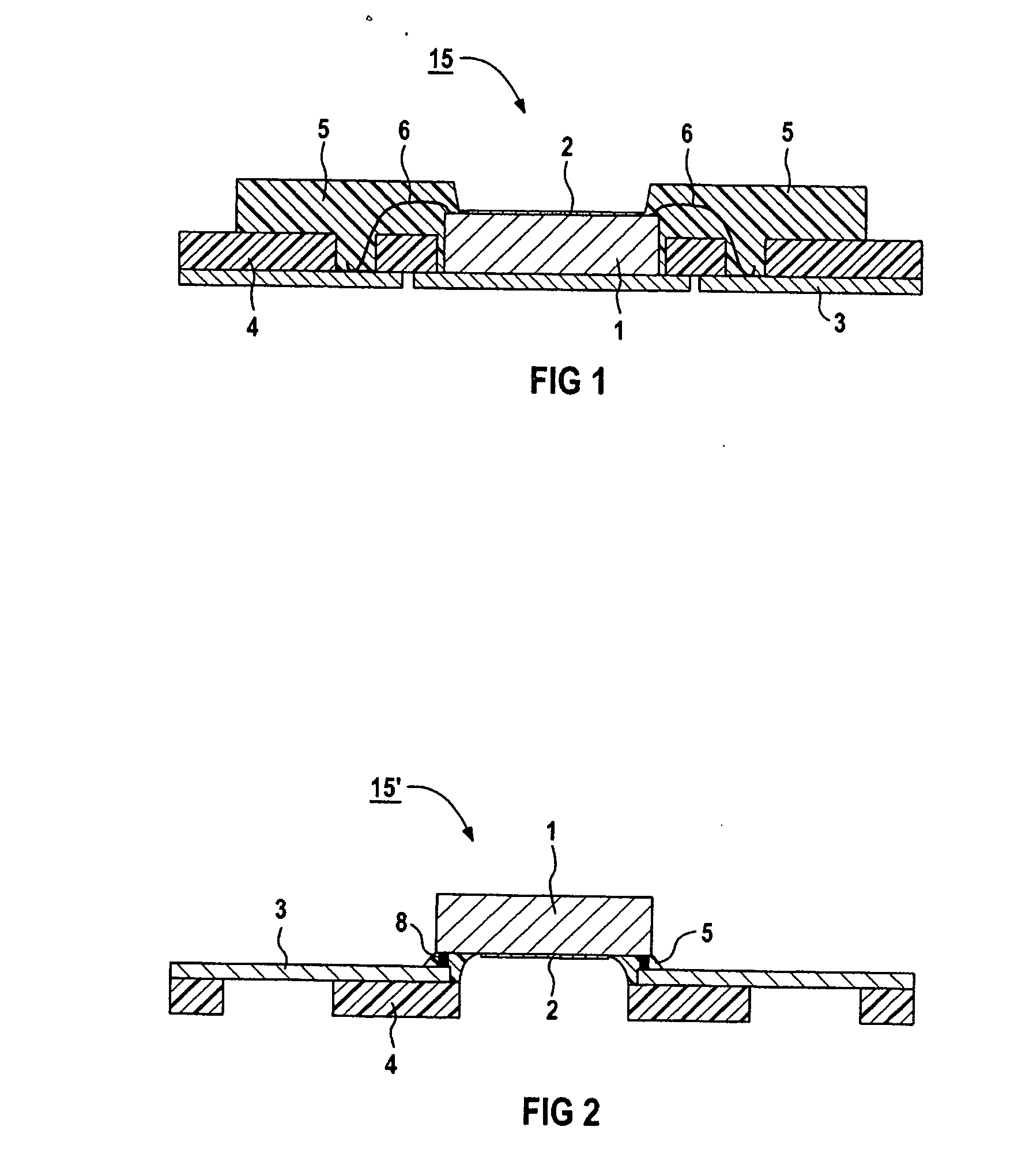
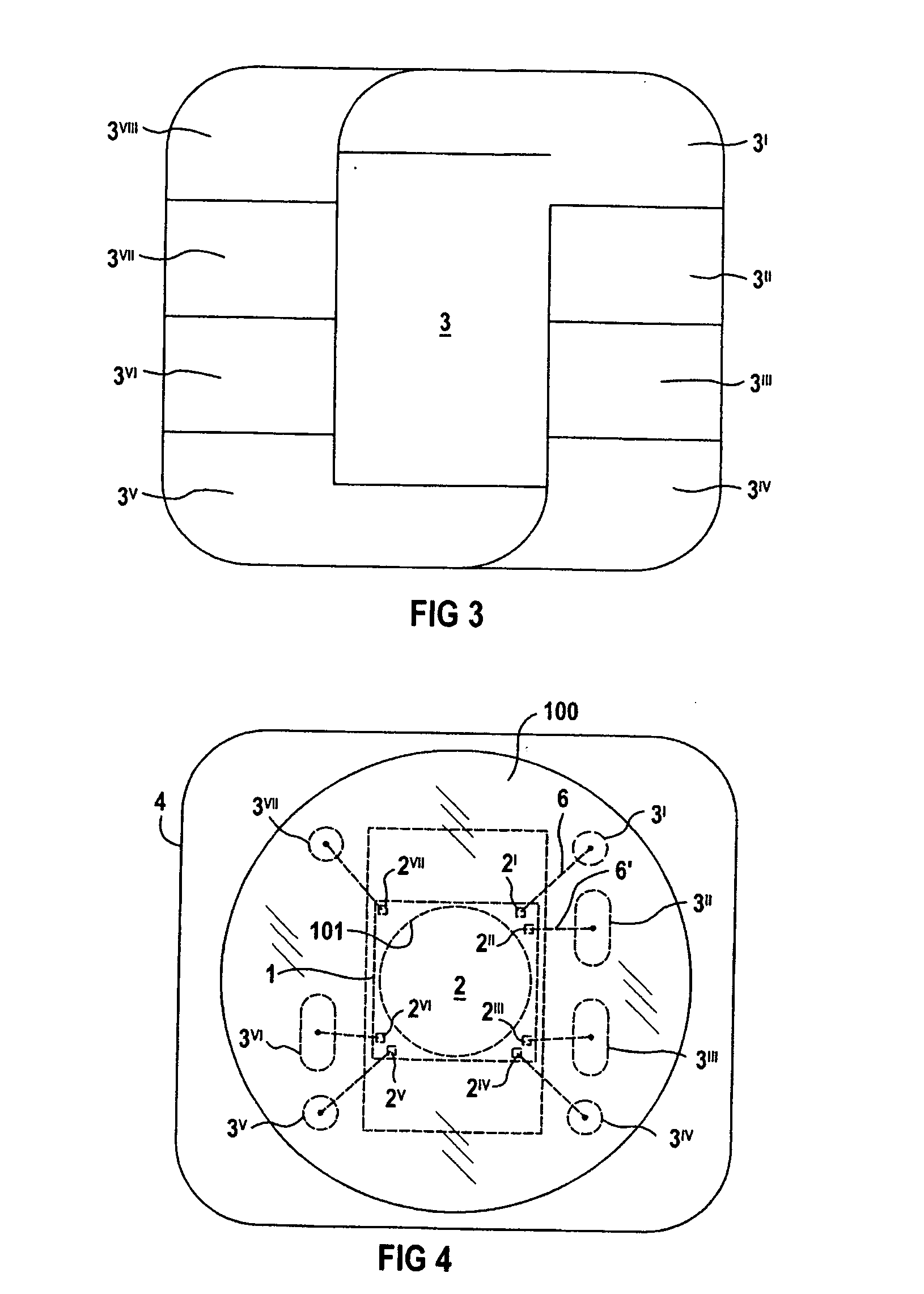
[0031] Chip card technology is a known, widespread and extremely low-cost housing concept in microelectronics. In this case, a microsilicon chip, which has previously being ground thin to about 180 μm at wafer level, is adhesively attached to a carrier strip, which may be a gold-coated, pre-punched copper strip and is possibly reinforced with a strip of plastic. After standard wire bonding, the chip together with the wires is encapsulated in a polymer. A commercially obtainable standard plastic card (materials: PVC, PET, PC; dimensions: about 85×54×0.8 mm3) is milled out at a defined location to module size (about 13×12×0.4 mm3) for receiving the chip carrier module, so that on...


PUM

PropertyMeasurementUnit
thicknessaaaaaaaaaa
thicknessaaaaaaaaaa
thicknessesaaaaaaaaaa

Abstract

An analysis device that may be used in biochemical analyses includes a module in a first housing, including a chip support, a sensor chip and electrical contacts between the chip and the chip support. The chip is encapsulated so that the electrical contacts are insulated and the sensitive surface of the sensor chip remains accessible to a fluid to be tested. The module and the first housing form an exchangeable applicator or chip card with mocrofluidic components or functions and is inserted into a second housing that has an evaluation unit for reading and analyzing measured data.

Description

CROSS REFERENCE TO RELATED APPLICATIONS [0001] This application is based on and hereby claims priority to German Application No. 101 11 458.3 filed on Mar. 9, 2001, the contents of which are hereby incorporated by reference. This application is related to ANALYSIS DEVICE, filed concurrently by Walter Gumbrecht and Manfred Stanzel and incorporated by reference herein. BACKGROUND OF THE INVENTION [0002] 1. Field of the Invention [0003] The invention relates to a module for an analysis device, in particular for decentralized biochemical analytics, with a sensor chip in a first housing. In addition, the invention also relates to an applicator as an exchangeable part of the analysis device and to the associated analysis device. [0004] 2. Description of the Related Art [0005] Microsensor technology and microsystems engineering have undergone a dramatic development in the last 20 years on the technological platform of microelectronics. All technical-scientific disciplines have made their r...

Claims


Application Information

Patent Timeline
Patent Type & Authority Applications(United States)
IPC IPC(8): B01L3/00G01N33/49C12M1/00G01N27/28G01N27/403G01N33/487G01N33/53G01N33/84G01N35/00G01N35/08G01N37/00
CPCB01L3/502707B01L3/502715B01L2200/027B01L2300/0645B01L2300/1805H01L2924/1815H01L2224/48091G01N27/128H01L2924/10253H01L2924/01068H01L2224/49171H01L2224/16H01L2924/00014H01L2924/00H01L2224/0401
Inventor GUMBRECHT, WALTERSTANZEL, MANFREDWOSSLER, MANFREDZAPF, JORG
Owner SIEMENS AG
Why Eureka
Try Eureka