Method and apparatus for controlling spatial distribution of RF power and plasma density

a technology of rf power and density, applied in the field of methods and apparatus for generating plasma, can solve the problems of non-uniform density distribution of plasma over the wafer, and achieve the effect of eliminating non-uniformity

Inactive Publication Date: 2005-02-10
TAIWAN SEMICON MFG CO LTD
View PDF3 Cites 61 Cited by
  • Summary
  • Abstract
  • Description
  • Claims
  • Application Information

AI Technical Summary

Benefits of technology

[0014] A still further object of the invention is to provide a method and apparatus of the type generally described above that is

Problems solved by technology

Unfortunately, however, the density distribution of the plasma is often not uniform over the wafer, but instead varies as a result of a number of factors, such as non uniform heating of the wafer, variations in the physical g

Method used


Image

  • Method and apparatus for controlling spatial distribution of RF power and plasma density
  • Method and apparatus for controlling spatial distribution of RF power and plasma density
  • Method and apparatus for controlling spatial distribution of RF power and plasma density

Examples


Embodiment Construction

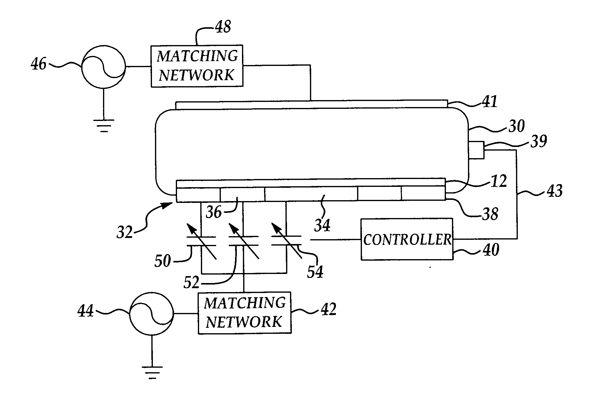
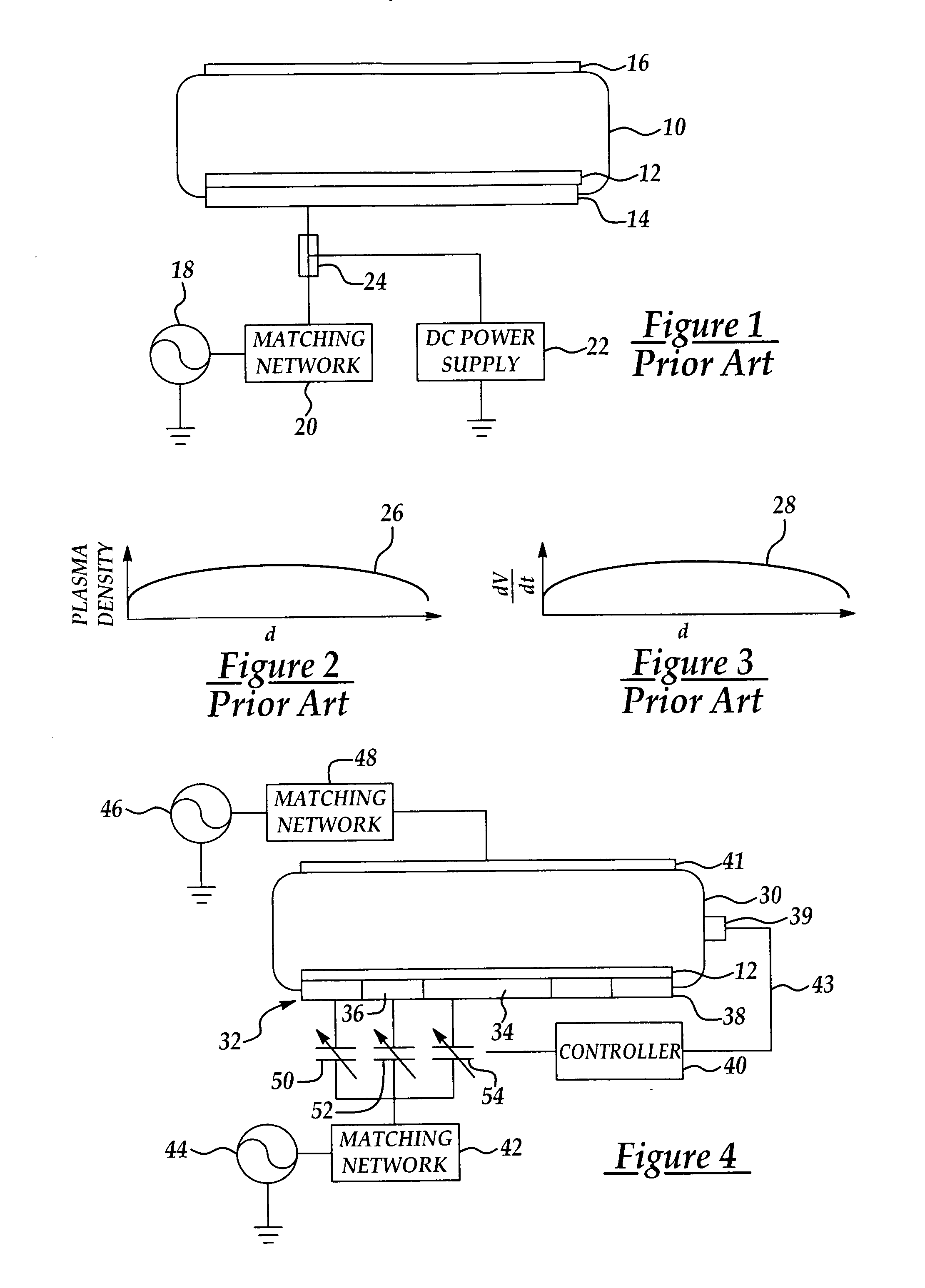
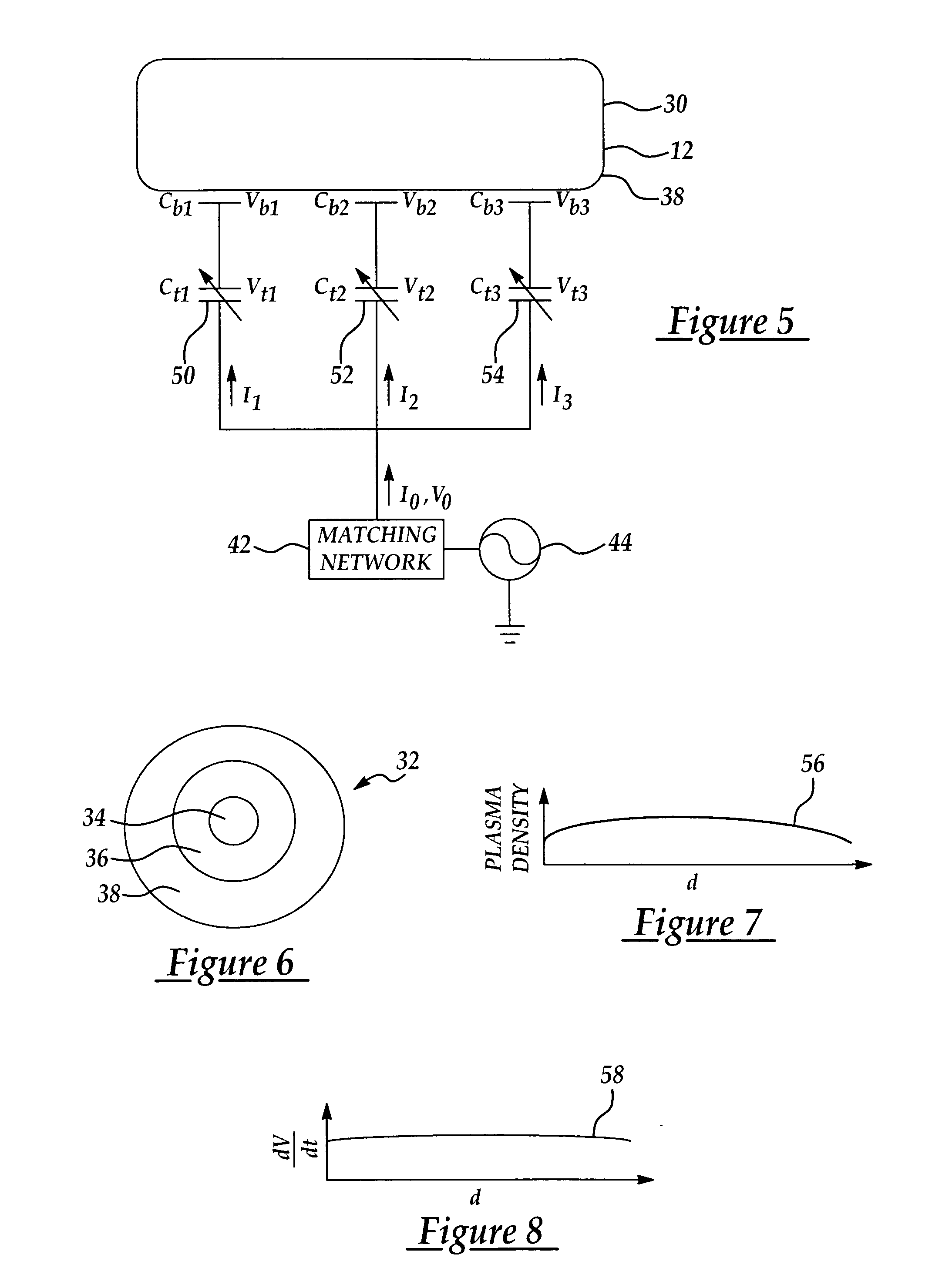
[0024] Referring first to FIG. 1, a conventional prior art, monopole ESC is depicted comprising a plate 14 for holding a semiconductor wafer 12 thereon within a processing chamber 10. The ESC plate 14 is connected to a DC power supply 22 using a DC / RF coupler 24. The wafer 12 is separated from the plate 14 by a thin layer of a dielectric (not shown). The DC power supply 22 charges the plate 14 which causes charge separation on the bottom surface of the wafer 12, resulting in the latter being attracted to and clamped to the plate 14. An RF electric field is created within the chamber 10 using a RF power source 18 which delivers RF power through a matching network 20 and the DC / RF coupler 24 to plate 14 which acts as a first electrode. The alternating voltage applied by the RF power source to the first electrode plate 14 is known as the RF bias voltage. A second electrode 16 cooperates with the electrode plate 14 to produce an electric field over the upper surface of the wafer 12 with...


PUM

PropertyMeasurementUnit
Poweraaaaaaaaaa
Densityaaaaaaaaaa
Electric potential / voltageaaaaaaaaaa

Abstract

Uniform spatial distribution of plasma over the face of a semiconductor wafer is achieved using a multi-zone electrode forming part of an electrostatic chuck used to hold the wafer in a processing chamber. The electrode includes a plurality of concentric electrode portions to which differing RF bias voltages may be applied to produce an electric field having a desired spatial distribution. Sensors are used to monitor either the spatial distribution of the plasma or the process effects of the plasma, and the sensed information is fed back to a controller that adjusts the bias voltage on the electrode portions in a manner to maintain the spatial uniformity of the plasma.

Description

TECHNICAL FIELD [0001] The present invention broadly relates to methods and apparatus for generating plasmas used to manufacture semiconductor devices, and deals more particularly with a technique for controlling the spatial distribution of RF power used to generate the plasma. BACKGROUND OF THE INVENTION [0002] In processing semiconductor wafers used to form integrated circuits, plasma-assisted processes are frequently used for both depositing materials onto the wafer and for etching materials from the wafer surface. Such processes include plasma etching, reactive ion etching (RIE), plasma enhanced chemical vapor deposition (PECVD), as well as a number of other well-known processes. In order to generate the plasma, an RF (radio frequency) power source is used to power to one or more electrodes within a vacuum vessel containing a gas at a predetermined pressure in which the processing is to take place. A matching network is typically used to efficiently couple power from the RF powe...

Claims


Application Information

Patent Timeline
IPC IPC(8): H01J37/32
CPCH01J37/32082H01J37/32935H01J37/32174
Inventor WU, SUNNYCHEN, BING-HUNGCHEN, PING-HSUCHANG, CHIH-TIEN
Owner TAIWAN SEMICON MFG CO LTD
Why Eureka
Try Eureka