Semiconductor device with improved protection from electrostatic discharge

a technology of electrostatic discharge and semiconductor devices, which is applied in the direction of semiconductor devices, semiconductor/solid-state device details, electrical apparatus, etc., can solve the problems of thermal damage and poor gate oxide quality at the corners, and achieve the effects of avoiding electric field concentration, avoiding gate-drain overlap, and improving protection from electrostatic discharg

Active Publication Date: 2005-02-17
LAPIS SEMICON CO LTD
View PDF9 Cites 5 Cited by
  • Summary
  • Abstract
  • Description
  • Claims
  • Application Information

AI Technical Summary

Benefits of technology

[0017] The invention provides improved protection from electrostatic discharge by avoiding gate-drain overlap in corner areas, thereby avoiding electric field concentration in areas where oxide quality is comparatively poor.
[0018] The second and third aspects of the invention simplify the design of the semiconductor device because the level of protection from electrostatic discharge depends linearly on the polygonal side dimensions of the device.
[0019] The third aspect of the invention also simplifies the design of the semiconductor device by providing added layout flexibility.

Problems solved by technology

If these diffusions 5, 9 are too close together, the parasitic diodes 10 may break down under ESD stress, leading to thermal damage as discharge current surges through the relatively small total diode width.
This problem is thought to result from electric field concentration combined with poor gate oxide quality at the corners 16.
The result of an oxide breakdown under ESD stress is often fatal to the device: the ESD current burns a hole through the oxide film.

Method used


Image

  • Semiconductor device with improved protection from electrostatic discharge
  • Semiconductor device with improved protection from electrostatic discharge
  • Semiconductor device with improved protection from electrostatic discharge

Examples


first embodiment

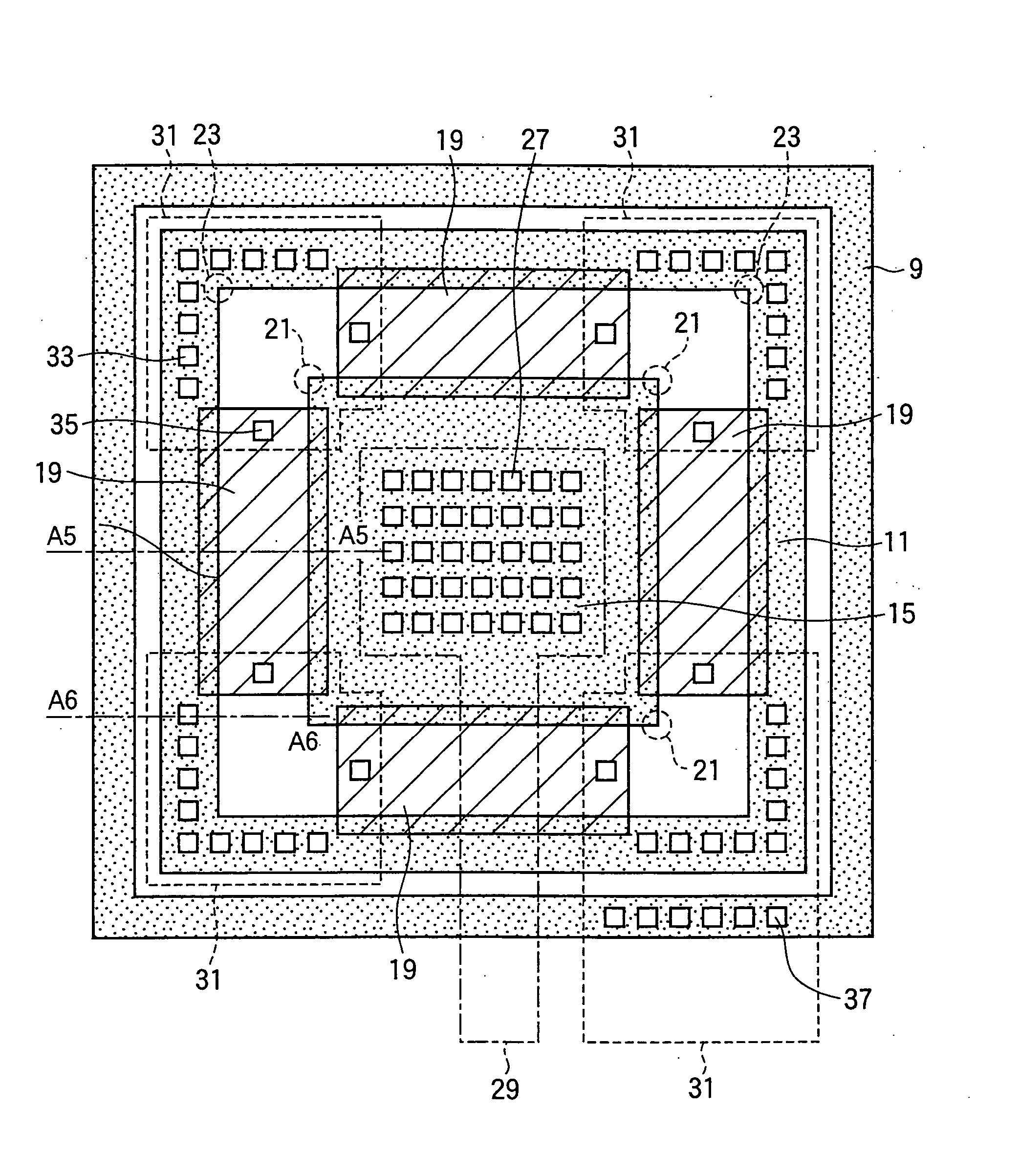
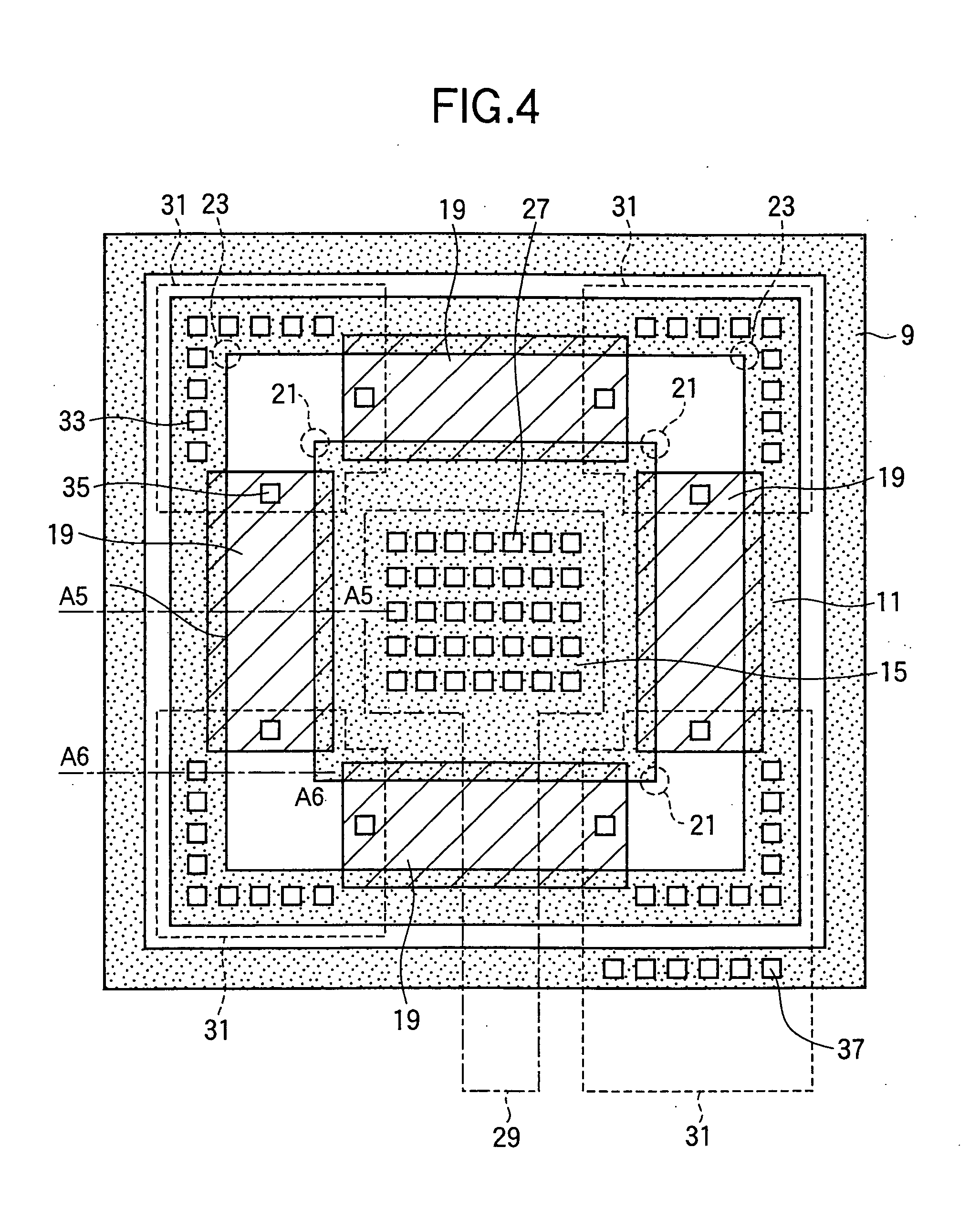
[0033] As the invention, FIGS. 4-6 show a field-effect transistor comprising a guard ring diffusion 9, a source diffusion 11., and a drain diffusion 15 formed in a silicon semiconductor substrate 17. As shown in FIG. 4, the drain diffusion 15 is square, the source diffusion 11 is a square annulus surrounding the drain diffusion 15, and the guard ring diffusion 9 is a square annulus surrounding the source diffusion 11.

[0034] Disposed between the four sides of the drain diffusion 15 and the facing sides of the source diffusion 11, and partially overlapping these sides, are four gate electrodes 19, each a rectangular body of polycrystalline silicon (polysilicon) formed on the substrate 17, insulated from the substrate 17 by an oxide film (not visible). The gate electrodes 19 do not overlap the corners 21 of the drain diffusion 15, or the corners 23 of the source diffusion 11. The substrate 17, diffusions 9, 11, 15, and gate electrode 19 are covered by an interlayer dielectric film 25 s...

second embodiment

[0040] As the invention, FIG. 7 shows a field-effect transistor comprising a guard ring diffusion 9, four source diffusions 43, and a drain diffusion 45 formed in a silicon semiconductor substrate. For an n-channel transistor, the source and drain diffusions 43, 45 are n-type with n+ and n− regions, the substrate is p-type, and the guard ring diffusion 9 is p+-type; for a p-channel transistor, the source and drain diffusions 43, 45 are p-type with p+ and p− regions, the substrate is n-type, and the guard ring diffusion 9 is n+-type. The drain diffusion 45 has the shape of a stubby square cross, that is, a square with the four corners removed. The source diffusions 43 are rectangles facing the four ends of the drain diffusion 45. The guard ring diffusion 9 is a square annulus surrounding the source diffusions 43.

[0041] The gate electrode 47 in this transistor has a square annular shape covering the four channel regions between the source diffusions 43 and the stubby ends of the drain...

third embodiment

[0045] As the invention, FIG. 11 shows a field-effect transistor comprising a guard ring diffusion 9, four source diffusions 43, and four drain diffusions 51 in a silicon semiconductor substrate. The source and drain diffusions 43, 51 are rectangular in shape. For an n-channel transistor, the source and drain diffusions 43, 51 are n-type with n+ and n− regions, the substrate is p-type, and the guard ring diffusion 9 is p+-type; for a p-channel transistor, the source and drain diffusions 43, 51 are p-type with p+ and p− regions, the substrate is n-type, and the guard ring diffusion 9 is n+-type. The four drain diffusions 51 substantially surround a central square area 52 in which no diffusion is formed, the drain diffusions 51 being longitudinally parallel to the four sides of the square. The four source diffusions 43 lie outside and face the four drain diffusions 51. The guard ring diffusion 9 is a square annulus surrounding the source diffusions 43.

[0046] Four gate electrodes 53 co...


PUM


Abstract

A concentric polygonal metal-oxide-semiconductor field-effect transistor is designed to avoid overlap between corners of the central drain diffusion and inner corners of the surrounding annular gate electrode. For example, the gate electrode may be reduced to separate straight segments by eliminating the corner portions. Alternatively, the drain diffusion may have a cross shape, and the outer annular source diffusion may be reduced to straight segments facing the ends of the cross, or the source and drain diffusions and gate electrodes may all be reduced to separate straight segments. By avoiding electric field concentration in the corner regions, these designs provide enhanced protection from electrostatic discharge.

Description

BACKGROUND OF THE INVENTION [0001] 1. Field of the Invention [0002] The present invention relates to a semiconductor device, and more particularly to a metal-oxide-semiconductor field-effect transistor with improved protection against electrostatic discharge. [0003] 2. Description of the Related Art [0004] The shrinking dimensions of complementary metal-oxide-semiconductor (CMOS) integrated circuits require special designs for transistors that conduct large amounts of current. Such transistors are found in particular in CMOS input and output circuits, where they are needed to drive heavy loads and to provide protection from electrostatic discharge (ESD). [0005] One known high-current transistor design is the finger design illustrated in FIG. 1, which places multiple gate electrodes 1 between an alternating series of source 3 and drain 5 diffusions. If the transistor is an n-channel metal-oxide-semiconductor (NMOS) transistor, for example, the source and drain diffusions 3, 5 are n-t...

Claims


Application Information

Patent Timeline
Patent Type & Authority Applications(United States)
IPC IPC(8): H01L23/528H01L23/58H01L23/60H01L23/62H01L29/06H01L29/417H01L29/78
CPCH01L23/5286H01L23/585H01L29/0619H01L29/0692H01L29/41725H01L2924/0002H01L29/78H01L2924/00
Inventor KURODA, TOSHIKAZUSASAKI, KATSUHITO
Owner LAPIS SEMICON CO LTD
Why Eureka
Try Eureka