

Thin film transistor, active matrix substrate, display device, and electronic apparatus
a technology of active matrix substrate and thin film transistor, which is applied in the direction of semiconductor devices, instruments, optics, etc., can solve the problems of difficult to secure reliability and difficult to suppress the deterioration of retention characteristics, and achieve the effect of high image quality and high precision
- Summary
- Abstract
- Description
- Claims
- Application Information
AI Technical Summary
Benefits of technology
Problems solved by technology
Method used
Image

Examples
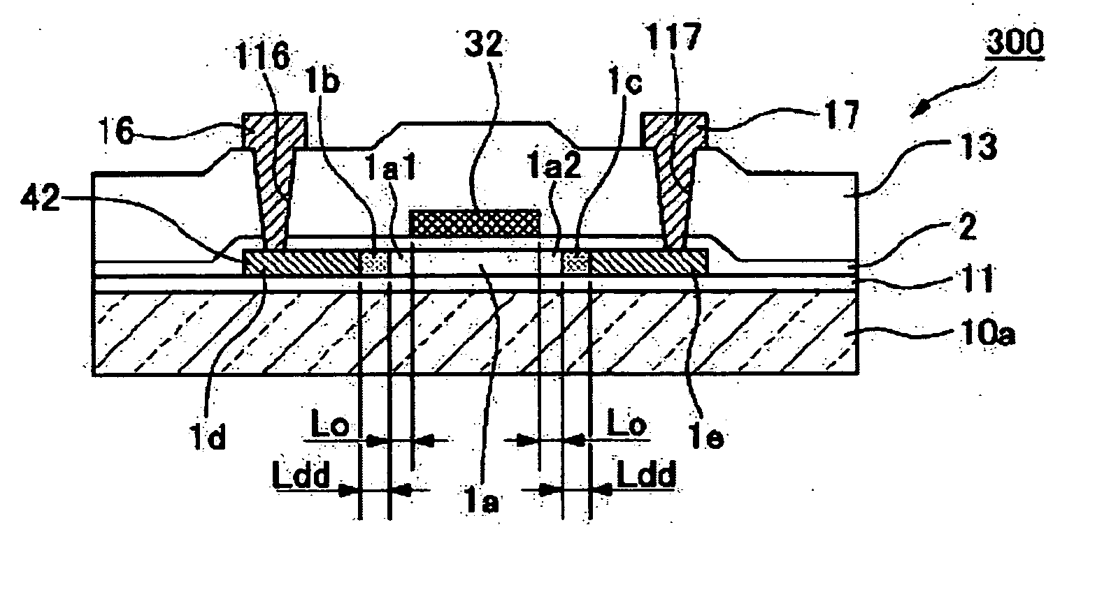
first exemplary embodiment
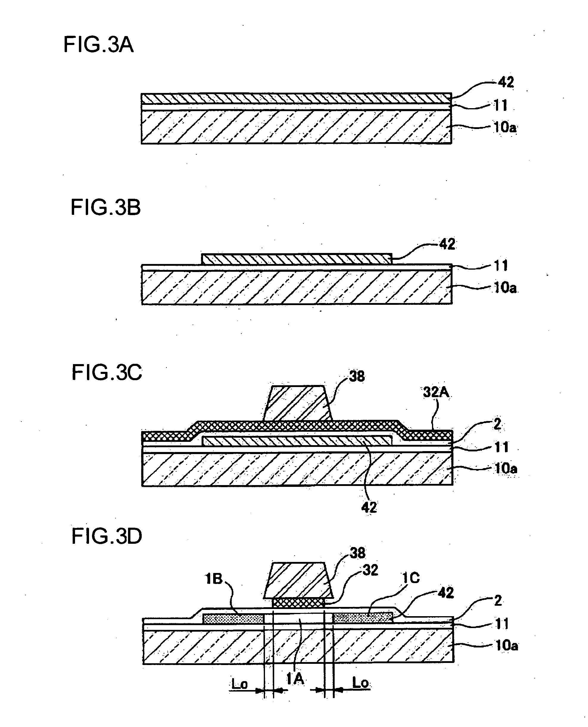
[0058] Next, a first exemplary embodiment of a method of manufacturing the thin film transistor according to an aspect of the present invention will be described. In this exemplary embodiment, a method of manufacturing the thin film transistor according to the aforementioned first exemplary embodiment will be described with reference to the figures. FIGS. 3 and 4 are schematics views illustrating processes of manufacturing the thin film transistor according to the first exemplary embodiment.
[0059] First, as shown in FIG. 3A, a silicon oxide film with a thickness of about 500 nm is formed as an underlying insulting film 11 on the substrate body 10a made of glass or quartz. Next, as shown in FIG. 3B, a semiconductor layer 42 being made of polysilicon is formed in an island shape on the underlying insulating film 11. The semiconductor layer 42 having an island shape may be formed by forming an amorphous silicon layer with a low hydrogen concentration on the underlying insulating film ...
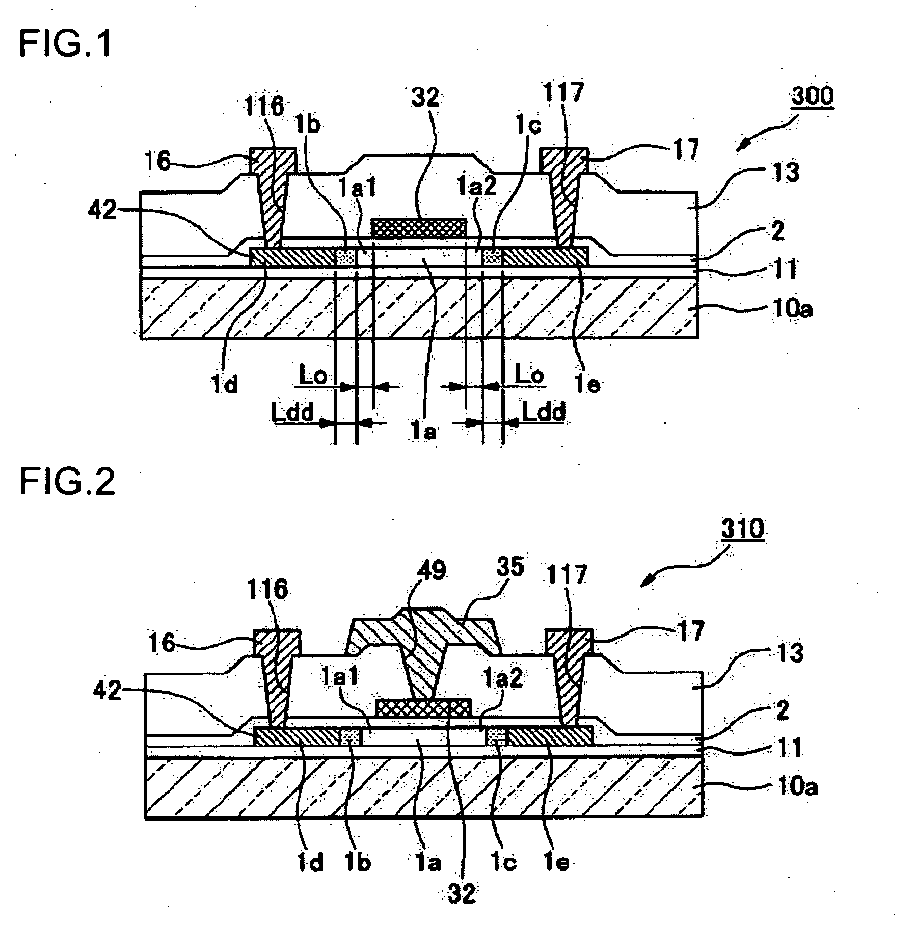
second exemplary embodiment
[0074] Next, a second exemplary embodiment of a method of manufacturing the thin film transistor according to an aspect of the present invention will be described with reference to FIGS. 11 and 12. FIGS. 11 and 12 are schematics illustrating processes of the manufacturing method according to this exemplary embodiment. In this exemplary embodiment, the method of manufacturing the thin film transistor according to the aforementioned first exemplary embodiment will be described, where the same constituent elements shown in FIGS. 11 and 12 as FIGS. 1 to 4 are denoted by the same reference numerals and descriptions thereof will be omitted.
[0075] First, as shown in FIG. 11A, a silicon oxide film with a thickness of about 500 mn is formed as an underlying insulting film 11 on the substrate body 10a made of glass or quartz. Next, as shown in FIG. 11B, a semiconductor layer 42 made of polysilicon is formed in an island shape on the underlying insulating film 11. The semiconductor layer 42 h...
PUM
| Property | Measurement | Unit |
|---|---|---|
| length | aaaaa | aaaaa |
| length | aaaaa | aaaaa |
| length | aaaaa | aaaaa |
Abstract
Description
Claims
Application Information